 ChipApex | Global Electronic Components Supplier
SEARCH
Search Product
Search Post
— IC芯片 | 连接器 | 传感器 | 被动器件 —
Search productSearch post
— IC芯片 | 连接器 | 传感器 | 被动器件 —
Consult the customer manager about the wholesale price.
consultation hotline:86-132-6715-2157
email:[email protected]
Contact the product manager for consultation. One-stop consultation is available.
Do you want a lower wholesale price? Please send us your inquiry and we will reply immediately.
The PI6C2410QE is a low skew, low jitter PLL clock buffer designed for PCI-X applications in servers and workstations. It features four synchronous outputs with selectable divider or multiplier ratios. The device accepts TTL input signals and provides TTL output signals. It operates within a supply voltage range of 3V to 3.6V and supports maximum frequencies of 133MHz for input and 66MHz for output. The component is housed in a 24-pin QSOP package and functions within an industrial temperature range of -40°C to +85°C.
Verify the specific package variant, as the 'Q' suffix denotes the 24-pin QSOP form factor. Confirm RoHS compliance status through official manufacturer documentation, as Pb-free and Green options are available across the series. Ensure the design accommodates the specified 3V to 3.6V supply voltage requirements.
Select this component when a low skew, low jitter PLL buffer is required for PCI-X environments. The device supports two selectable input frequency ranges (10-40 MHz and 40-80 MHz) determined by the HF# pin state. Verify that the application requires TTL logic levels for both input and output signals before integration.
The PI6C2410 belongs to the PCI-X Clock Buffers category from Diodes Incorporated. It is part of a family that includes variants such as the PI6C2410L (TSSOP package). The device was originally developed by Pericom Semiconductor Corporation before being acquired by Diodes Incorporated.
The PI6C2410L serves as a package-compatible alternative offering the same electrical specifications in a 24-pin TSSOP footprint. No other direct functional substitutes are documented in the provided source material.
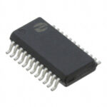 PI6C2410QE
The activity of extra discounts on wholesale prices is in full swing…
Please fill in your contact information and we will send you the latest wholesale price list.





