 ChipApex | Global Electronic Components Supplier

SEARCH
Search Product
Search Post
— IC芯片 | 连接器 | 传感器 | 被动器件 —
Search productSearch post
— IC芯片 | 连接器 | 传感器 | 被动器件 —
Consult the customer manager about the wholesale price.
consultation hotline:86-132-6715-2157
email:[email protected]
Contact the product manager for consultation. One-stop consultation is available.
Do you want a lower wholesale price? Please send us your inquiry and we will reply immediately.
PI6C4921502TQ1ZHWEX is listed in the Clock Buffers, Drivers range at ChipApex. The manufacturer field lists Diodes Incorporated. Its product description is CLOCK BUFFER W-QFN5050-32 T&R 2.. Review the specifications below when checking this part for your BOM.
The PI6C4921502TQ1ZHWEX is an automotive-grade high-performance LVDS fanout buffer manufactured by Diodes Incorporated. It provides two differential LVDS outputs organized into a single bank, supporting input frequencies up to 1.5 GHz. The device accepts LVPECL, LVDS, HCSL, CML, CMOS, or crystal inputs and features selectable reference inputs for single-ended, differential, or crystal sources. It includes a separate LVCMOS reference output capable of reaching 200 MHz. Electrical specifications include a core supply voltage range of 2.375 V to 3.465 V and an ambient operating temperature range from -40°C to +125°C.
Verify that the specific ordering suffix matches the required package and qualification level. The 'ZHW' suffix indicates a 32-contact W-QFN5050-32 package. The '1' in the part number denotes AEC-Q100 Grade 1 qualification. Confirm the 'X' suffix corresponds to Tape/Reel packaging if reel delivery is required. Ensure the design supports the specified -40°C to +125°C operating temperature range.
Select this component when a low-jitter clock distribution solution is required for automotive environments. The PI6C4921502TQ1ZHWEX is suitable for designs needing two differential LVDS outputs. If four outputs are required instead of two, consider the PI6C4921504 variant within the same family. Verify that the input signal type matches the supported formats: LVDS, LVPECL, HCSL, CML, CMOS, or Crystal.
This device belongs to the PI6C492150xTQ product line, which consists of high-performance automotive LVDS fanout buffers. The family includes variants with different output counts, such as the PI6C4921504TQ1ZHWEX, which provides four LVDS outputs. All members of this series share similar electrical characteristics, including ultra-low jitter and support for various input logic levels, while maintaining AEC-Q100 Grade 1 compliance.
The PI6C4921504TQ1ZHWEX is a confirmed substitute within the same family offering four outputs instead of two. Both parts share the ZHW package and AEC-Q100 Grade 1 qualification. No other cross-model substitutes are documented in the provided datasheet.
Explore related parts through Clock/Timing, Integrated Circuits (ICs), all product categories, ChipApex homepage.
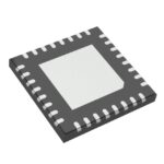 PI6C4921502TQ1ZHWEX

The activity of extra discounts on wholesale prices is in full swing…
Please fill in your contact information and we will send you the latest wholesale price list.






