 ChipApex | Global Electronic Components Supplier

SEARCH
Search Product
Search Post
— IC芯片 | 连接器 | 传感器 | 被动器件 —
Search productSearch post
— IC芯片 | 连接器 | 传感器 | 被动器件 —
Consult the customer manager about the wholesale price.
consultation hotline:86-132-6715-2157
email:[email protected]
Contact the product manager for consultation. One-stop consultation is available.
Do you want a lower wholesale price? Please send us your inquiry and we will reply immediately.
PI6C49CB01Q3WEX is listed in the Clock Buffers, Drivers range at ChipApex. The manufacturer field lists Diodes Incorporated. Its product description is IC CLK TRANSLTR 1:1 360MHZ 8SOIC. Review the specifications below when checking this part for your BOM.
The PI6C49CB01Q3WEX is a 1-to-1 Differential-to-LVCMOS/LVTTL Translator High Performance Buffer manufactured by Diodes Incorporated. It accepts differential inputs including LVPECL, LVDS, LVHSTL, SSTL, and HCSL, converting them to a single-ended LVCMOS or LVTTL output. The device operates on a supply voltage of 2.375 V to 3.465 V with an output frequency up to 360 MHz. Propagation delay ranges from 1.6 ns to 2.5 ns depending on the supply voltage. It is AEC-Q100 qualified for Grade 3 automotive applications (-40°C to +85°C) and housed in an 8-pin SOIC package.
Verify that the ordering suffix '3' corresponds to the required -40°C to +85°C temperature range. Confirm the 'WEX' suffix indicates the 8-pin Wide SOIC package and Tape/Reel packaging format. Ensure compliance with RoHS and Halogen-free requirements as specified in the datasheet notes.
Select this component when a single-ended LVCMOS or LVTTL output is needed from various differential clock sources. The 360 MHz maximum frequency supports high-speed digital interfaces. Consider the 500 ps part-to-part skew specification for multi-device synchronization requirements within the system design.
This part belongs to the PI6C49CB01Q family of automotive-qualified buffers. The '3' suffix specifically denotes the Grade 3 temperature rating (-40°C to +85°C), distinguishing it from the Grade 2 variant which supports up to +105°C. Both variants share identical electrical characteristics but differ in thermal qualification.
The PI6C49CB01Q2WEX serves as a direct functional substitute if the application requires the extended temperature range of -40°C to +105°C (Automotive Grade 2). Electrical parameters remain consistent between the two variants.
The device supports a maximum output frequency of 360 MHz.
At 3.3V, the maximum propagation delay is 2.0 ns. At 2.5V, the maximum propagation delay increases to 2.5 ns.
Yes, the differential input can be wired to accept single-ended levels using external bias resistors and capacitors to generate a reference voltage of VDD/2.
Explore related parts through Clock/Timing, Integrated Circuits (ICs), all product categories, ChipApex homepage.
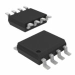 PI6C49CB01Q3WEX

The activity of extra discounts on wholesale prices is in full swing…
Please fill in your contact information and we will send you the latest wholesale price list.






