 ChipApex | Global Electronic Components Supplier

SEARCH
Search Product
Search Post
— IC芯片 | 连接器 | 传感器 | 被动器件 —
Search productSearch post
— IC芯片 | 连接器 | 传感器 | 被动器件 —
Consult the customer manager about the wholesale price.
consultation hotline:86-132-6715-2157
email:[email protected]
Contact the product manager for consultation. One-stop consultation is available.
Do you want a lower wholesale price? Please send us your inquiry and we will reply immediately.
PI6C49S1506FAIEX is listed in the Clock Buffers, Drivers range at ChipApex. The manufacturer field lists Diodes Incorporated. Its product description is IC CLK BUFFER 3:6 1.5GHZ 32TQFP. Review the specifications below when checking this part for your BOM.
The PI6C49S1506FAIEX is a high-performance differential fanout buffer from Diodes Incorporated, housed in a 32-pin TQFP package. It supports output frequencies up to 1.5 GHz with six differential outputs organized into two configurable banks. The device allows per-bank selection of LVPECL, LVDS, or HCSL signaling standards and accepts single-ended, differential, or crystal inputs. Key electrical parameters include a typical propagation delay of 1.5 ns, intra-bank skew under 40 ps, and ultra-low additive phase jitter below 0.03 ps (typical). It operates on separate VDD and VDDO supplies ranging from 2.375 V to 3.465 V within an industrial temperature range of -40°C to +85°C.
Verify the ordering suffix 'EX' corresponds to tape and reel packaging as indicated in the datasheet notes. Confirm that the specific revision matches the required electrical characteristics. Ensure supply voltage levels align with the selected output standard, as VDD and VDDO may require independent regulation for level shifting compatibility.
Select this component when distributing high-speed differential clocks with mixed interface requirements across different system sections. The dual-bank architecture allows mixing LVPECL and LVDS outputs on the same device. Consider the separate power supply pins (VDD/VDDO) for noise isolation and ensure adequate decoupling capacitors are placed near the pins to maintain jitter performance.
This part belongs to the PI6C49S1506 series of high-performance fanout buffers manufactured by Diodes Incorporated (formerly Pericom). The FAIE suffix indicates a lead-free, green RoHS-compliant device in a 32-pin TQFP package. The 'X' suffix denotes tape and reel packaging for automated assembly.
Check pin-to-pin compatibility with existing designs if substituting other PI6C49 series devices. Verify that alternative buffers support the same configurable output standards and frequency range up to 1.5 GHz. Ensure thermal and mechanical dimensions match the TQFP-32 footprint.
Explore related parts through Clock/Timing, Integrated Circuits (ICs), all product categories, ChipApex homepage.
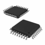 PI6C49S1506FAIEX

The activity of extra discounts on wholesale prices is in full swing…
Please fill in your contact information and we will send you the latest wholesale price list.





