 ChipApex | Global Electronic Components Supplier

SEARCH
Search Product
Search Post
— IC芯片 | 连接器 | 传感器 | 被动器件 —
Search productSearch post
— IC芯片 | 连接器 | 传感器 | 被动器件 —
Consult the customer manager about the wholesale price.
consultation hotline:86-132-6715-2157
email:[email protected]
Contact the product manager for consultation. One-stop consultation is available.
Do you want a lower wholesale price? Please send us your inquiry and we will reply immediately.
PI6C49S1510BZDIEX is listed in the Clock Buffers, Drivers range at ChipApex. The manufacturer field lists Diodes Incorporated. Its product description is IC CLK BUFFER 3:10 1.5GHZ 48TQFN. Review the specifications below when checking this part for your BOM.
The PI6C49S1510BZDIEX is a high-performance fanout buffer from Diodes Incorporated, designed for distributing low jitter clock signals to multiple destinations. It supports differential output frequencies up to 1.5 GHz and features user-configurable signaling standards (LVDS, LVPECL, or HCSL) across two independent output banks. The device integrates an ultra-low additive phase jitter of less than 0.02 ps (typical) at 156.25 MHz. It accepts single-ended, differential, or crystal reference inputs and includes a separate LVCMOS reference output capable of reaching 200 MHz. Operating within a -40°C to +85°C temperature range, it utilizes a 48-pin TQFN package.
Verify the specific ordering suffix 'ZDIEX' corresponds to the 48-pin TQFN package and tape/reel packaging format as defined in the datasheet. Confirm that the component meets RoHS 3 compliance and halogen-free requirements if environmental specifications are critical for the intended assembly process.
Select this component when flexible output interface levels are required across different destination devices within the same system. Ensure the input source matches one of the supported types: differential, single-ended, or crystal oscillator. Verify that the power supply voltage range of 2.375V to 3.465V aligns with the system design constraints.
This part belongs to the PI6C49S1510 family of high-performance differential fanout buffers. The ZD suffix indicates the 48-contact Very Thin Quad Flat No-Lead (TQFN) package. The I suffix denotes industrial temperature support, while E signifies lead-free and green manufacturing processes compliant with EU directives.
Direct replacements within the same series include variants with different package codes or output configurations, such as the PI6C49S1510AZDIEX. Verify pin compatibility and electrical parameters before substitution.
The output signaling standard for each bank (A and B) is configured via the OPMODEA and OPMODEB input pins. These pins select between LVPECL, LVDS, HCSL, or Hi-Z states.
The device supports three reference input types selected by the IN_SEL pins: Differential (IN0+/IN0- or IN1+/IN1-), Single-ended (X1), or Crystal Oscillator (X1/X2).
The LVCMOS reference output (Ref_Out) can operate at frequencies up to 200 MHz when driven by a reference input, or up to 50 MHz when driven by a crystal input.
Explore related parts through Clock/Timing, Integrated Circuits (ICs), all product categories, ChipApex homepage.
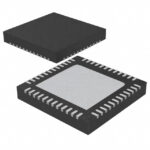 PI6C49S1510BZDIEX

The activity of extra discounts on wholesale prices is in full swing…
Please fill in your contact information and we will send you the latest wholesale price list.





