 ChipApex | Global Electronic Components Supplier

SEARCH
Search Product
Search Post
— IC芯片 | 连接器 | 传感器 | 被动器件 —
Search productSearch post
— IC芯片 | 连接器 | 传感器 | 被动器件 —
Consult the customer manager about the wholesale price.
consultation hotline:86-132-6715-2157
email:[email protected]
Contact the product manager for consultation. One-stop consultation is available.
Do you want a lower wholesale price? Please send us your inquiry and we will reply immediately.
PI6C49X0204CWIEX is listed in the Clock Buffers, Drivers range at ChipApex. The manufacturer field lists Diodes Incorporated. Its product description is IC CLK BUFFER 1:4 200MHZ 8SOIC. Review the specifications below when checking this part for your BOM.
The PI6C49X0204CWIEX is a low skew, single-input to four-output clock buffer manufactured by Diodes Incorporated. It utilizes low power CMOS technology and operates within an industrial temperature range of -40°C to +85°C. The device supports supply voltages from 1.425V to 3.6V. Key electrical specifications include a maximum propagation delay of 5ns at 1.5V and 2.5ns at 3.3V, with output-to-output skew limited to ±250ps. The input clock pin is 3.6V tolerant, and the unit is housed in an 8-pin Wide SOIC package.
Verify the component against the official datasheet DS43291 Rev 1-2 to confirm technical parameters. Ensure the ordering suffix matches the required package and reel specifications. Confirm compliance with RoHS and halogen-free requirements as defined by the manufacturer's quality definitions before procurement.
Select this component for designs requiring low skew distribution of a single clock signal to four destinations. Verify that the operating voltage falls within the 1.425V to 3.6V range. Consider the 3.6V tolerant input if interfacing with higher voltage logic levels. Ensure the PCB layout accommodates the 8-pin Wide SOIC package dimensions.
This part belongs to the PI6C49X series of clock buffers from Diodes Incorporated. The specific model PI6C49X0204C provides a 1:4 fanout ratio. The 'W' indicates the Wide SOIC package, and 'IE' denotes lead-free and green packaging. It is distinct from other variants in the series that may offer different output counts or package types.
Direct replacements must match the 1:4 fanout ratio, 8-pin Wide SOIC package, and compatible voltage ranges. Verify pin compatibility and electrical characteristics such as propagation delay and skew. Consult the manufacturer for automotive qualified alternatives if AEC-Q100 compliance is required.
The Output Enable (OE) pin controls the state of the outputs. When the OE pin is pulled low, all four outputs are tri-stated.
Yes, the CLK input pin is specified as 3.6V tolerant, allowing it to interface with higher voltage logic levels while the device operates at lower supply voltages.
The maximum output-to-output skew is ±250ps, measured between any two outputs with equal loading at rising edges at VDD/2.
Explore related parts through Clock/Timing, Integrated Circuits (ICs), all product categories, ChipApex homepage.
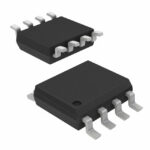 PI6C49X0204CWIEX

The activity of extra discounts on wholesale prices is in full swing…
Please fill in your contact information and we will send you the latest wholesale price list.




