 ChipApex | Global Electronic Components Supplier
SEARCH
Search Product
Search Post
— IC芯片 | 连接器 | 传感器 | 被动器件 —
Search productSearch post
— IC芯片 | 连接器 | 传感器 | 被动器件 —
Consult the customer manager about the wholesale price.
consultation hotline:86-132-6715-2157
email:[email protected]
Contact the product manager for consultation. One-stop consultation is available.
Do you want a lower wholesale price? Please send us your inquiry and we will reply immediately.
The PI6CDBL401BZHIE is a 4-output low power buffer designed for PCIe Gen1, Gen2, and Gen3 applications. It features an integrated Zero-Delay Buffer (ZDB) PLL and provides four differential outputs compatible with HCSL or LVDS standards. The device operates on a core supply voltage of 3.3V ±10% and supports output supply voltages of 1.8V, 2.5V, or 3.3V. It includes programmable output amplitude and slew rate settings via SMBus, along with individual output enables. The component is housed in a 32-TQFN package and supports industrial ambient operating temperatures ranging from -40°C to +85°C.
Verify that the ordering suffix matches the required packaging format. The 'E' suffix indicates lead-free and green material compliance, while the 'X' suffix specifies tape and reel packaging. Confirm the specific package code ZH32 corresponds to the 32-contact Thin Quad Flat No-Lead form factor required for the target PCB layout.
Select this component when a low-power solution for PCIe clock distribution is required. Ensure the design accommodates separate VDDO supply rails if utilizing 1.8V or 2.5V output levels. Verify that the input clock source meets the specified differential swing and slew rate requirements for reliable operation within the industrial temperature range.
This part belongs to the PI6CDBL401B series manufactured by Diodes Incorporated. It serves as a specialized clock buffer within the company's portfolio of application-specific timing solutions. The device integrates control logic and a zero-delay buffer to manage clock signals efficiently in multi-lane PCIe architectures.
Public confirmed substitute part numbers are not available in the provided documentation.
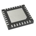 PI6CDBL401BZHIE
The activity of extra discounts on wholesale prices is in full swing…
Please fill in your contact information and we will send you the latest wholesale price list.





