 ChipApex | Global Electronic Components Supplier
SEARCH
Search Product
Search Post
— IC芯片 | 连接器 | 传感器 | 被动器件 —
Search productSearch post
— IC芯片 | 连接器 | 传感器 | 被动器件 —
Consult the customer manager about the wholesale price.
consultation hotline:86-132-6715-2157
email:[email protected]
Contact the product manager for consultation. One-stop consultation is available.
Do you want a lower wholesale price? Please send us your inquiry and we will reply immediately.
The PI6CDBL401BZHIEX is a 4-output low power buffer designed for PCIe Gen1, Gen2, and Gen3 applications. It features an integrated zero-delay buffer (ZDB) PLL and provides four differential outputs compatible with HCSL or LVDS standards. The device operates on a core supply voltage of 3.3V ±10% and supports output supply voltages of 1.8V, 2.5V, or 3.3V. It accepts a differential clock input up to 400 MHz in bypass mode or 100 MHz in PLL mode. Key electrical parameters include a maximum propagation delay of 4.5 ns in bypass mode and cycle-to-cycle jitter of 50 ps in PLL mode at 100 MHz. The component is housed in a 32-TQFN package.
Verify the ordering suffix ZHIEX corresponds to the 32-TQFN package with Tape & Reel packaging. Confirm RoHS compliance and lead-free status as indicated by the 'E' suffix in the base part number. Ensure the specific revision (Rev 4-2) matches design requirements. Check for any Product Change Notifications (PCN) related to manufacturing site or material changes before finalizing procurement.
Select this component when designing PCIe interfaces requiring a 1:4 fan-out buffer with low power consumption. Ensure the target application supports the required output voltage range (1.8V to 3.3V). Verify that the input clock source meets the differential voltage swing and slew rate specifications. Consider the SMBus interface requirements for configuring output enables and PLL modes during system initialization.
The PI6CDBL401B belongs to Diodes Incorporated's family of low-power clock buffers. The ZHIEX suffix denotes the specific tape and reel packaging configuration for the 32-contact Thin Quad Flat No-Lead (TQFN) package. This variant is optimized for surface mount assembly in high-density PCB layouts typical of modern computing platforms.
Public confirmed substitute part numbers are not available in the provided documentation. Designers should consult Diodes Incorporated for current alternative recommendations if this specific part number becomes unavailable.
The PI6CDBL401B supports three PLL modes: High Bandwidth (HiBW), Bypass, and Low Bandwidth (LoBW), selected via the HIBW_BYPM_LOBW# pin or SMBus commands.
The device offers three selectable SMBus addresses determined by the state of the SADR_tri pin upon the first assertion of CKPWRGD_PD#.
Yes, the outputs are LVDS compatible. External termination resistors may be required depending on whether the receiving LVDS input has internal termination.
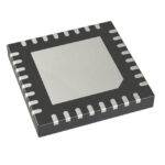 PI6CDBL401BZHIEX
The activity of extra discounts on wholesale prices is in full swing…
Please fill in your contact information and we will send you the latest wholesale price list.




