 ChipApex | Global Electronic Components Supplier
SEARCH
Search Product
Search Post
— IC芯片 | 连接器 | 传感器 | 被动器件 —
Search productSearch post
— IC芯片 | 连接器 | 传感器 | 被动器件 —
Consult the customer manager about the wholesale price.
consultation hotline:86-132-6715-2157
email:[email protected]
Contact the product manager for consultation. One-stop consultation is available.
Do you want a lower wholesale price? Please send us your inquiry and we will reply immediately.
The PI6CDBL402BLIE is a PCIe 3.0 compliant, low-power differential clock buffer designed as a companion to PCIe 3.0 clock generators. It distributes a differential SRC clock input to four differential pairs of outputs in either PLL or bypass mode. The device supports independent output power supplies ranging from 1.8V to 3.3V and operates on a 3.3V core supply. Key electrical parameters include a maximum bypass frequency of 400 MHz and a typical cycle-to-cycle jitter of 45 ps at 100 MHz. It features an SMBus interface for configuration and is housed in a 28-TSSOP package.
Verify the ordering suffix 'E' confirms Pb-free and Green compliance. Confirm the package type matches the 28-TSSOP specification. Ensure the design supports the required voltage levels for VDDA and VDDO. Check for specific tape and reel requirements if applicable.
Select this component when a low-power, multi-output buffer is needed for PCIe applications. Consider the 1.8V to 3.3V output supply flexibility for mixed-voltage systems. Evaluate the SMBus requirement for dynamic configuration against simpler hardware-controlled alternatives.
This part belongs to the PI6CDBL402B series of low-power PCIe buffers. It is manufactured by Diodes Incorporated, formerly Pericom Semiconductor. The device is specifically engineered to meet the stringent jitter and power requirements of modern high-speed serial interfaces.
Direct replacements within the same family include PI6CDBL402BLIEX (Tape & Reel variant). Verify pinout compatibility and electrical specifications before substituting with other clock buffer models.
The device supports independent output power supplies (VDDO) ranging from 1.8V to 3.3V.
PLL operation is selected via the PLL/BYPASS# pin or through the SMBus interface.
The maximum operating frequency in bypass mode is 400 MHz.
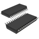 PI6CDBL402BLIE
The activity of extra discounts on wholesale prices is in full swing…
Please fill in your contact information and we will send you the latest wholesale price list.





