 ChipApex | Global Electronic Components Supplier
SEARCH
Search Product
Search Post
— IC芯片 | 连接器 | 传感器 | 被动器件 —
Search productSearch post
— IC芯片 | 连接器 | 传感器 | 被动器件 —
Consult the customer manager about the wholesale price.
consultation hotline:86-132-6715-2157
email:[email protected]
Contact the product manager for consultation. One-stop consultation is available.
Do you want a lower wholesale price? Please send us your inquiry and we will reply immediately.
The PI6CDBL402BLIEX is a PCIe 3.0 compliant, low-power differential clock buffer designed to distribute SRC clocks from PCIe generators. It supports backward compatibility with PCIe 1.0 and 2.0 specifications. The device features a 1:4 fan-out ratio with four differential output pairs (HCSL/LVDS). It operates with a core supply voltage of 3.0V to 3.6V and an independent output supply range of 1.62V to 3.63V. Key electrical parameters include a typical cycle-to-cycle jitter of 45ps at 100MHz in bypass mode and less than 1ps additive RMS phase jitter. The component utilizes a 28-TSSOP package.
Verify the ordering suffix 'X' confirms the Tape & Reel packaging format. Confirm that the specific revision matches the required RoHS compliance status. Ensure the 28-TSSOP footprint dimensions align with the PCB layout design rules before finalizing procurement orders.
Select this component when a low-skew (<60ps) differential buffer is required for PCIe applications. The independent VDDO supply allows optimization for different output voltage levels (1.8V, 2.5V, or 3.3V). Verify that the input clock frequency falls within the 1-400MHz bypass range or requires the 100MHz PLL mode.
This part belongs to the PI6CDBL402B series of low-power PCIe buffers. The 'E' suffix indicates Pb-free and Green manufacturing compliance. The 'X' suffix specifically denotes the Tape & Reel packaging variant, distinguishing it from the tube-packaged version.
Public confirmed substitute part numbers are not available in the provided documentation.
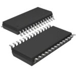 PI6CDBL402BLIEX
The activity of extra discounts on wholesale prices is in full swing…
Please fill in your contact information and we will send you the latest wholesale price list.





