 ChipApex | Global Electronic Components Supplier
SEARCH
Search Product
Search Post
— IC芯片 | 连接器 | 传感器 | 被动器件 —
Search productSearch post
— IC芯片 | 连接器 | 传感器 | 被动器件 —
Consult the customer manager about the wholesale price.
consultation hotline:86-132-6715-2157
email:[email protected]
Contact the product manager for consultation. One-stop consultation is available.
Do you want a lower wholesale price? Please send us your inquiry and we will reply immediately.
The PI6CEQ20200LE is a PCIe Gen2/Gen3 zero-delay buffer featuring two HCSL outputs. It incorporates internal equalization to enhance signal integrity for long-distance clock distribution. The device operates on a 3.135V to 3.465V supply with a maximum frequency of 110MHz. Key electrical specifications include cycle-to-cycle jitter of 40ps typical and output-to-output skew under 10ps. It supports dual PLL bandwidth selection for spread-spectrum clocking tracking and includes SMBus control capabilities.
Verify the ordering suffix against the manufacturer's datasheet to confirm package type and temperature range. The 'LE' suffix indicates a Pb-free, Green 20-pin TSSOP package with a commercial operating temperature range of 0°C to 70°C. Confirm whether tape-and-reel packaging is required by checking for an additional 'X' suffix in the part number.
Select this component for applications requiring low-jitter clock buffering for PCIe Gen2 or Gen3 interfaces. Ensure the design environment stays within the commercial temperature range of 0°C to 70°C. For industrial temperatures (-40°C to 85°C), consider the LI variant. Verify that the system requires HCSL output levels and SMBus configuration support.
This component belongs to the Pericom PI6CEQ series of high-performance clock buffers. It is designed specifically to meet the stringent jitter and signal integrity requirements of PCI Express standards. The device integrates equalization techniques to compensate for channel loss, making it suitable for complex motherboard layouts.
Public confirmed substitute part numbers are not available in the provided documentation.
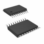 PI6CEQ20200LE
The activity of extra discounts on wholesale prices is in full swing…
Please fill in your contact information and we will send you the latest wholesale price list.






