 ChipApex | Global Electronic Components Supplier
SEARCH
Search Product
Search Post
— IC芯片 | 连接器 | 传感器 | 被动器件 —
Search productSearch post
— IC芯片 | 连接器 | 传感器 | 被动器件 —
Consult the customer manager about the wholesale price.
consultation hotline:86-132-6715-2157
email:[email protected]
Contact the product manager for consultation. One-stop consultation is available.
Do you want a lower wholesale price? Please send us your inquiry and we will reply immediately.
The PI6CEQ20200LIE is a PCIe Gen2/Gen3 zero-delay buffer manufactured by Diodes Incorporated. It features one HCSL differential input and two HCSL differential outputs, operating within a supply voltage range of 3.135V to 3.465V. The device supports input frequencies up to 110MHz and functions in an industrial temperature range of -40°C to +85°C. Key electrical specifications include a typical cycle-to-cycle jitter of 40ps and output-to-output skew under 10ps. It utilizes internal equalization for signal integrity and is housed in a 20-TSSOP package.
Verify the ordering suffix 'I' confirms the -40°C to +85°C industrial temperature rating. Confirm whether the 'X' suffix is required for tape-and-reel packaging or if bulk quantities are available without it. Ensure the component is sourced from authorized distributors to guarantee authenticity and proper RoHS compliance documentation.
Select this part when a single HCSL source must drive multiple PCIe Gen2/Gen3 destinations with low skew. Verify that the system requires the specific 3.3V supply voltage range and SMBus interface capabilities. Consider the 20-TSSOP footprint constraints during PCB layout design.
This component belongs to the PI6CEQ20200 series of high-performance clock buffers. The 'LIE' suffix specifically denotes the Pb-free, Green compliant version packaged in a 20-pin TSSOP with extended industrial temperature support (-40°C to +85°C).
Check datasheets for other PI6CEQ20200 variants such as PI6CEQ20200LE (commercial temp) or PI6CEQ20200LEX (reel). Ensure any substitute maintains the same HCSL I/O standards and SMBus compatibility.
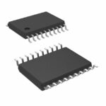 PI6CEQ20200LIE
The activity of extra discounts on wholesale prices is in full swing…
Please fill in your contact information and we will send you the latest wholesale price list.






