 ChipApex | Global Electronic Components Supplier
SEARCH
Search Product
Search Post
— IC芯片 | 连接器 | 传感器 | 被动器件 —
Search productSearch post
— IC芯片 | 连接器 | 传感器 | 被动器件 —
Consult the customer manager about the wholesale price.
consultation hotline:86-132-6715-2157
email:[email protected]
Contact the product manager for consultation. One-stop consultation is available.
Do you want a lower wholesale price? Please send us your inquiry and we will reply immediately.
The PI6CEQ20200LIEX is a PCIe Gen2/Gen3 zero-delay buffer manufactured by Diodes Incorporated, housed in a 20-TSSOP package. It features one HCSL differential input and two HCSL differential outputs with a 1:2 ratio. The device operates on a 3.135V to 3.465V supply within an industrial temperature range of -40°C to +85°C. Key electrical parameters include a maximum frequency of 110MHz, cycle-to-cycle jitter of 40ps typical, and output-to-output skew under 10ps. It integrates internal equalization for signal integrity improvement.
Verify the ordering suffix 'E' confirms Pb-free and Green status, while 'X' indicates Tape & Reel packaging. Confirm the 'I' suffix matches the required -40°C to +85°C industrial temperature grade. Ensure the 20-TSSOP (0.173 inch width) package dimensions align with the PCB footprint requirements before finalizing procurement orders.
Select this component when designing PCIe Gen2 or Gen3 interfaces requiring low skew and high signal integrity over long traces. The dual PLL bandwidth selection allows optimization for specific spread-spectrum clocking frequencies. Ensure the design accommodates the 3.3V supply voltage and provides adequate thermal dissipation for the TSSOP-20 package within the specified ambient temperature limits.
This part belongs to the PI6CEQ series of PCIe clock buffers produced by Diodes Incorporated (formerly Pericom). It serves as a specialized timing solution for high-speed serial interfaces, replacing standard oscillators or buffers that lack integrated equalization and zero-delay buffering capabilities required for modern PCIe compliance.
Public confirmed substitute part numbers are not available in the provided documentation. Verify pinout compatibility and electrical specifications against alternative PCIe clock generators if sourcing from different manufacturers.
The PLL_BW_SEL pin selects the PLL loop bandwidth. A logic high sets a high bandwidth (1.3MHz to 3MHz), while a logic low sets a low bandwidth (0.25MHz to 1MHz).
Outputs are controlled by OE_0# and OE_1# pins. A logic low enables the respective outputs, while a logic high tri-states them. These pins have internal pull-down resistors.
In bypass mode, where the PLL is disabled, the maximum propagation delay is 4.0 ns.
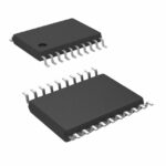 PI6CEQ20200LIEX
The activity of extra discounts on wholesale prices is in full swing…
Please fill in your contact information and we will send you the latest wholesale price list.





