 ChipApex | Global Electronic Components Supplier
SEARCH
Search Product
Search Post
— IC芯片 | 连接器 | 传感器 | 被动器件 —
Search productSearch post
— IC芯片 | 连接器 | 传感器 | 被动器件 —
Consult the customer manager about the wholesale price.
consultation hotline:86-132-6715-2157
email:[email protected]
Contact the product manager for consultation. One-stop consultation is available.
Do you want a lower wholesale price? Please send us your inquiry and we will reply immediately.
The PI6CFGL201B is a 2-output low-power clock generator designed for PCIe Gen 1, 2, and 3 applications. It generates a maximum frequency of 100MHz from a 25MHz crystal or reference input. The device features integrated output terminations (Zo=100Ω) and supports HCSL, LVDS, and LVCMOS outputs. Key electrical parameters include a supply voltage range of 3V to 3.6V, an operating temperature range of -40°C to +85°C, and cycle-to-cycle jitter typically around 30ps. It includes spread spectrum capabilities (-0.25%, -0.5%) and programmable slew rates.
Verify the package type matches the required form factor; the standard reel version carries the 'X' suffix (PI6CFGL201BZDIEX). Confirm that the design accommodates the 24-TQFN exposed pad connection to ground for thermal management. Ensure the SMBus address configuration aligns with system requirements before finalizing procurement.
Select this component when a low-power solution for PCIe Gen 1-3 is required. It supports both crystal and external reference clock inputs. Verify that the load capacitance requirements for the connected crystal (typically CL=18pF) are met by the external capacitors. Check if the specific spread spectrum level needed is supported by hardware pins or software control.
This part belongs to the PI6CFGL series of low-power clock generators from Diodes Incorporated. It is functionally similar to other models in the family but specifically configured for 2 outputs at up to 100MHz. It serves as a direct replacement for legacy Pericom devices in PCIe clocking designs.
Public confirmed substitute part numbers are not available in the provided documentation.
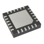 PI6CFGL201BZDIEX
The activity of extra discounts on wholesale prices is in full swing…
Please fill in your contact information and we will send you the latest wholesale price list.





