 ChipApex | Global Electronic Components Supplier
SEARCH
Search Product
Search Post
— IC芯片 | 连接器 | 传感器 | 被动器件 —
Search productSearch post
— IC芯片 | 连接器 | 传感器 | 被动器件 —
Consult the customer manager about the wholesale price.
consultation hotline:86-132-6715-2157
email:[email protected]
Contact the product manager for consultation. One-stop consultation is available.
Do you want a lower wholesale price? Please send us your inquiry and we will reply immediately.
The PI6CFGL401BZHIEX is a four-output low-power clock generator designed for PCI Express Gen1, Gen2, and Gen3 applications. It features an integrated spread-spectrum capable PLL and provides four differential HCSL outputs with built-in 100Ω terminations. The device accepts a 25MHz crystal or reference clock input and operates on a 3.3V supply voltage (3.0V to 3.6V) with a 1.8V output supply range (1.05V to 3.3V). Key electrical parameters include a maximum operating frequency of 100MHz, cycle-to-cycle jitter of approximately 30ps typical, and phase jitter compliant with PCIe specifications. It supports selectable spread spectrum levels of -0.25%, -0.5%, or no spread.
Verify the package type matches the required PCB footprint, as this component uses a 32-TQFN exposed pad. Confirm that the design supports the specific SMBus address selection via the SADR pin and the spread spectrum configuration via the SS_EN_tri pin at power-up. Ensure the board layout accounts for the separate analog and digital ground planes specified in the datasheet.
Select this component when designing for PCIe Gen1 through Gen3 interfaces requiring low power consumption and integrated output termination. It is suitable for systems needing configurable spread spectrum to reduce EMI. Verify that the application can accommodate the 32-TQFN package and provides the necessary 3.3V and 1.8V supply rails. Consider the SMBus interface requirements for dynamic configuration if needed.
This part belongs to the PI6CFGL series of low-power PCIe clock generators from Diodes Incorporated (formerly Pericom). It is specifically engineered to meet the stringent jitter and power requirements of modern PCI Express standards while minimizing board space through integrated terminations and a compact TQFN package.
Direct replacements within the same family include the PI6CFGL401BZHIE (non-reel version). For different output counts or PCIe generations, consult other parts in the PI6CG or PI6CDBL series, ensuring compatibility with the specific PCIe version and output interface requirements.
The device supports three spread spectrum modes: -0.25%, -0.5%, and Spread Off. The mode is selected via the SS_EN_tri pin at power-up or configured via SMBus.
The SMBus address is latched based on the state of the SADR pin when CKPWRGD_PD# is first asserted high. A logic low sets the address to 1101000, and a logic high sets it to 1101010.
Yes, the datasheet provides application notes for driving LVDS inputs, specifying external termination resistors (R7a/b and R8a/b) and coupling capacitors depending on whether the receiver has internal termination.
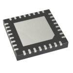 PI6CFGL401BZHIEX
The activity of extra discounts on wholesale prices is in full swing…
Please fill in your contact information and we will send you the latest wholesale price list.





