 ChipApex | Global Electronic Components Supplier
SEARCH
Search Product
Search Post
— IC芯片 | 连接器 | 传感器 | 被动器件 —
Search productSearch post
— IC芯片 | 连接器 | 传感器 | 被动器件 —
Consult the customer manager about the wholesale price.
consultation hotline:86-132-6715-2157
email:[email protected]
Contact the product manager for consultation. One-stop consultation is available.
Do you want a lower wholesale price? Please send us your inquiry and we will reply immediately.
The PI6CVF857AE is a PLL-based clock driver designed for registered DDR DIMM applications. It functions as a zero-delay buffer, distributing one differential clock input pair (CLK, CLK) to ten differential output pairs (Yx, Yx) and one feedback pair (FBOUT, FBOUT). The device operates at 2.5V for PC1600/PC2100/PC2700 and 2.6V for PC3200 standards. It supports operating frequencies up to 220 MHz with an application frequency range of 71–220 MHz. Key electrical parameters include a maximum cycle-to-cycle jitter of 50 fs, static phase offset of 50 ps, and output skew of 75 ps.
Verify the package type matches the required PCB footprint, as the PI6CVF857 series includes both TSSOP and QFN variants. Confirm the voltage requirements align with the target DDR generation (2.5V vs 2.6V). Check RoHS compliance status if environmental regulations apply to the specific manufacturing batch.
Select this component for designs requiring low-jitter clock distribution to multiple DDR memory modules. Ensure the input clock frequency falls within the 71–220 MHz application range. Verify that the system can accommodate the external feedback loop connections required for the zero-delay buffer operation.
This part belongs to the PI6CVF857 family of PLL clock drivers manufactured by Diodes Incorporated (formerly Pericom). It is specifically engineered for high-speed memory interfaces, providing precise timing synchronization for registered DIMMs in desktop and server platforms.
Public confirmed substitute part numbers are not available in the provided documentation.
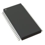 PI6CVF857AE
The activity of extra discounts on wholesale prices is in full swing…
Please fill in your contact information and we will send you the latest wholesale price list.






