 ChipApex | Global Electronic Components Supplier
SEARCH
Search Product
Search Post
— IC芯片 | 连接器 | 传感器 | 被动器件 —
Search productSearch post
— IC芯片 | 连接器 | 传感器 | 被动器件 —
Consult the customer manager about the wholesale price.
consultation hotline:86-132-6715-2157
email:[email protected]
Contact the product manager for consultation. One-stop consultation is available.
Do you want a lower wholesale price? Please send us your inquiry and we will reply immediately.
The PI6LC4840ZHE is a crystal-to-LVDS/LVCMOS frequency synthesizer designed for Ethernet applications. It operates on a 3.3V supply and supports 25MHz and 125MHz frequencies. The device features three output banks: Bank A provides pin-selectable 25/50MHz LVCMOS outputs, Bank B offers 125MHz LVCMOS outputs, and Bank C delivers 125MHz LVDS outputs. An additional non-PLL 25MHz LVCMOS reference clock output is available. Integrated phase noise is specified at a maximum of 1ps (12k-20MHz) for the 125MHz outputs.
Verify component authenticity through authorized Diodes Incorporated channels. Confirm RoHS compliance status and check for Product Change Notifications (PCN) regarding package or labeling updates prior to procurement.
Select this model when both LVCMOS and LVDS outputs are required simultaneously. Ensure the design accommodates the specific mode pin configurations for Bank A frequency selection. Verify that the external crystal matches the recommended load capacitance of 18pF.
This part belongs to the PI6LC48 family of clock generators. The 'ZH' suffix indicates the 32-contact TQFN package, while 'E' denotes Pb-free and Green manufacturing. It serves as a direct replacement for earlier Pericom Semiconductor Corporation designs under the Diodes Incorporated portfolio.
Check for PCN documents related to the PI6LC48 series. Verify if newer revisions maintain identical electrical characteristics and pinout compatibility before substituting.
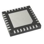 PI6LC4840ZHE
The activity of extra discounts on wholesale prices is in full swing…
Please fill in your contact information and we will send you the latest wholesale price list.





