 ChipApex | Global Electronic Components Supplier
SEARCH
Search Product
Search Post
— IC芯片 | 连接器 | 传感器 | 被动器件 —
Search productSearch post
— IC芯片 | 连接器 | 传感器 | 被动器件 —
Consult the customer manager about the wholesale price.
consultation hotline:86-132-6715-2157
email:[email protected]
Contact the product manager for consultation. One-stop consultation is available.
Do you want a lower wholesale price? Please send us your inquiry and we will reply immediately.
The PI6LC48H04LIE is a clock generator compliant with PCI Express® 4.0/3.0/2.0/1.0 and Ethernet standards, designed for networking or embedded systems. It accepts a 25MHz crystal input and generates four pairs of differential Low Power HCSL outputs at selectable frequencies: 156.25MHz, 100MHz, 125MHz, 133.33MHz, and 200MHz. The device operates on 3.3V±5% or 2.5V±5% supplies within an industrial temperature range (-40°C to +85°C). Key electrical parameters include a typical cycle-to-cycle jitter of 35ps and PCIe 4.0 RMS phase jitter of 0.45ps (typical) at 100MHz.
Verify the ordering suffix 'E' confirms lead-free and green status, and 'X' indicates tape and reel packaging. Confirm the package code 'L' corresponds to the 20-pin TSSOP form factor. Ensure the component meets RoHS 3 compliance requirements for your specific manufacturing process.
Select this part when multiple differential HCSL clocks are required from a single 25MHz reference. Verify that the target system supports the available output frequencies (100MHz, 125MHz, 156.25MHz, 200MHz) via S0/S1 pin configuration. Ensure the PCB layout accommodates the 20-TSSOP package dimensions.
This component belongs to the PI6LC48 family of clock generators from Diodes Incorporated. It is specifically engineered to meet the stringent jitter requirements of modern high-speed serial interfaces like PCIe Gen 4.0 while maintaining compatibility with legacy PCIe generations.
Publicly confirmed substitute part numbers are not provided in the source material. Consult Diodes Incorporated directly for alternative components or updated revisions.
The maximum RMS phase jitter for PCIe 4.0 is 0.45ps (typical 0.37ps), measured using a PLL bandwidth of 2-4MHz or 2-5MHz with a CDR of 10MHz.
Output frequencies are selected using the S0 and S1 input pins. For a 25MHz crystal input, S1=0/S0=0 yields 156.25MHz, S1=0/S0=1 yields 100MHz, S1=1/S0=0 yields 125MHz, and S1=1/S0=1 yields 200MHz.
Yes, the datasheet describes driving LVDS inputs using external termination resistors (R7a/b and R8a/b) and coupling capacitors (Cc) to match impedance and voltage levels.
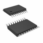 PI6LC48H04LIE
The activity of extra discounts on wholesale prices is in full swing…
Please fill in your contact information and we will send you the latest wholesale price list.





