 ChipApex | Global Electronic Components Supplier
SEARCH
Search Product
Search Post
— IC芯片 | 连接器 | 传感器 | 被动器件 —
Search productSearch post
— IC芯片 | 连接器 | 传感器 | 被动器件 —
Consult the customer manager about the wholesale price.
consultation hotline:86-132-6715-2157
email:[email protected]
Contact the product manager for consultation. One-stop consultation is available.
Do you want a lower wholesale price? Please send us your inquiry and we will reply immediately.
The PI6LC48P25104LE is a single-output LVPECL clock synthesizer from the HiFlex family, designed for Ethernet reference clock generation. It operates on 3.3V or 2.5V supplies and accepts a 25MHz crystal input to produce 156.25MHz or 187.5MHz outputs via Freq_SEL configuration. The device utilizes proprietary low phase noise PLL technology, achieving typical RMS phase jitter of 0.3ps at 156.25MHz (12kHz-20MHz). Packaged in an 8-pin TSSOP, it supports commercial temperature ranges.
Verify component authenticity through authorized Diodes Incorporated channels. Confirm package marking matches the ordering code PI6LC48P25104LE for lead-free green 8-pin TSSOP. Check datasheet revisions for any updates regarding thermal characteristics or packaging changes before finalizing procurement specifications.
Select this component when a single-ended LVPECL clock source is required for high-speed networking or storage interfaces. Ensure the design accommodates separate VDD and VDDA power pins with appropriate filtering (0.1μF bypass capacitors) to maintain specified jitter performance. Verify that the system environment falls within the commercial operating temperature range (-40°C to +85°C).
This part belongs to the Pericom HiFlex family of clock solutions, now manufactured by Diodes Incorporated following their acquisition. The PI6LC48P25104 specifically targets Ethernet reference clock generation, offering a compact alternative to discrete oscillator solutions while providing programmable frequency multiplication via external crystal inputs.
No direct public substitute part numbers are documented in the provided datasheet. Designers requiring replacement should evaluate other HiFlex series clock generators with compatible LVPECL outputs and similar frequency ranges, ensuring pinout compatibility or implementing necessary PCB redesigns.
The output frequency is determined by the Freq_SEL pin state. When Freq_SEL is LOW, the output is multiplied by 6.25 (yielding 156.25MHz with a 25MHz crystal). When HIGH, it is multiplied by 7.5 (yielding 187.5MHz).
The device supports full 3.3V or 2.5V supply modes. VDD (core) and VDDA (analog) must be individually connected to the power plane with 0.1μF bypass capacitors. For optimal jitter performance, VDDA requires an additional 10Ω resistor and 10μF capacitor.
Using a 25MHz crystal, the typical RMS phase jitter is 0.3ps at 156.25MHz and 0.33ps at 187.5MHz, measured over the 12kHz to 20MHz offset frequency range.
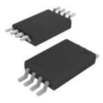 PI6LC48P25104LE
The activity of extra discounts on wholesale prices is in full swing…
Please fill in your contact information and we will send you the latest wholesale price list.






