 ChipApex | Global Electronic Components Supplier

SEARCH
Search Product
Search Post
— IC芯片 | 连接器 | 传感器 | 被动器件 —
Search productSearch post
— IC芯片 | 连接器 | 传感器 | 被动器件 —
Consult the customer manager about the wholesale price.
consultation hotline:86-132-6715-2157
email:[email protected]
Contact the product manager for consultation. One-stop consultation is available.
Do you want a lower wholesale price? Please send us your inquiry and we will reply immediately.
PI6ULS5V9517AWE is listed in the Signal Buffers, Repeaters, Splitters range at ChipApex. The manufacturer field lists Diodes Incorporated. Its product description is IC REDRIVER I2C 1CH 400KHZ 8SOIC. Review the specifications below when checking this part for your BOM.
The PI6ULS5V9517AWE is a CMOS integrated circuit designed for I2C-bus and SMBus applications, functioning as a level translating repeater. It provides bidirectional buffering for serial data (SDA) and clock (SCL) lines across two channels. Port A operates with a supply voltage range of 0.8 V to 5.5 V, while Port B operates from 2.2 V to 5.5 V. The device supports Standard-mode and Fast-mode devices up to 400 kHz. It features an active HIGH enable input, open-drain outputs, and ESD protection exceeding 8 kV HBM. The WE suffix indicates the SOIC-8 package.
Verify the specific ordering suffix 'WE' corresponds to the SOIC-8 package when sourcing components. Confirm that the manufacturer has not designated this package type as 'Not Recommended for New Design' for current projects. Ensure compliance with RoHS and lead-free requirements specified in the datasheet notes before finalizing procurement specifications.
Select this component when interfacing I2C buses with significantly different supply voltages, specifically where one side drops below 2.2 V. Ensure the application requires bidirectional buffering for both SDA and SCL lines. Verify that the operating frequency does not exceed the repeater's propagation delay limitations at the target speed.
This part belongs to the PI6ULS5V9517 family of level translating repeaters manufactured by Diodes Incorporated. The base model PI6ULS5V9517 is available in MSOP-8, TDFN2x3-8, and SOIC-8 packages. The WE designation specifically identifies the SOIC-8 variant, which is noted by the manufacturer as not recommended for new designs compared to other package options.
PI6ULS5V9517AZEEX (TDFN2x3-8 package)
Yes, multiple devices can be connected in series, provided that Port A of one device is connected to Port B of the next. This configuration allows for extended bus topologies limited only by timing constraints.
Changing the EN pin state during an active bus cycle should be avoided. Disabling the repeater mid-operation can hang the bus, while enabling it partially through a cycle may confuse the connected I2C devices.
The device is designed for lock-up free operation. Specifically, the Port B internal buffer maintains a buffered low level that prevents the input from recognizing its own output as a valid low, avoiding feedback loops.
Explore related parts through Interface, Integrated Circuits (ICs), all product categories, ChipApex homepage.
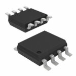 PI6ULS5V9517AWE

The activity of extra discounts on wholesale prices is in full swing…
Please fill in your contact information and we will send you the latest wholesale price list.





