 ChipApex | Global Electronic Components Supplier

SEARCH
Search Product
Search Post
— IC芯片 | 连接器 | 传感器 | 被动器件 —
Search productSearch post
— IC芯片 | 连接器 | 传感器 | 被动器件 —
Consult the customer manager about the wholesale price.
consultation hotline:86-132-6715-2157
email:[email protected]
Contact the product manager for consultation. One-stop consultation is available.
Do you want a lower wholesale price? Please send us your inquiry and we will reply immediately.
PL123-02NGC-R is listed in the Clock Buffers, Drivers range at ChipApex. The manufacturer field lists Microchip Technology. Its product description is IC CLK BUFFER 1:2 200MHZ 6DFN. Review the specifications below when checking this part for your BOM.
The PL123-02NGC-R is a low-cost, general-purpose 1:2 inverting LVCMOS fanout buffer manufactured by Microchip Technology. It supports operating frequencies up to 200 MHz at 3.3V, 150 MHz at 2.5V, and 100 MHz at 1.8V. The device features an Output Enable (OE) pin that allows disabling outputs into an active-low state, reducing power consumption to less than 5 µA. It accepts SST and non-SST clock signals with Spread Spectrum Modulation. The component operates within a supply voltage range of 1.62 V to 3.63 V and is housed in a space-saving 6-lead UDFN package.
Verify the ordering suffix 'R' indicates a 3,000/Reel media type as specified in the Product Identification System. Confirm the 'C' suffix corresponds to the commercial temperature range of 0°C to +70°C. Ensure compatibility with the 6-Lead UDFN package dimensions before procurement.
Select this model for applications requiring a 1:2 inverting fanout buffer with an enable function. Choose based on required operating frequency relative to the supply voltage (e.g., 200 MHz requires 3.3V). Verify the commercial temperature range (0°C to +70°C) meets system requirements; use the 'I' suffix variant for industrial ranges (-40°C to +85°C).
This part belongs to the PL123-02N series, which includes variants with different temperature ratings and packaging options. The 'G' denotes the 6-Lead UDFN package, while 'C' specifies the commercial temperature grade. The '-R' suffix designates the tape and reel packaging format.
Public confirmed substitute part numbers are not available in the provided source material.
Explore related parts through Clock/Timing, Integrated Circuits (ICs), all product categories, ChipApex homepage.
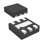 PL123-02NGC-R

The activity of extra discounts on wholesale prices is in full swing…
Please fill in your contact information and we will send you the latest wholesale price list.




