 ChipApex | Global Electronic Components Supplier

SEARCH
Search Product
Search Post
— IC芯片 | 连接器 | 传感器 | 被动器件 —
Search productSearch post
— IC芯片 | 连接器 | 传感器 | 被动器件 —
Consult the customer manager about the wholesale price.
consultation hotline:86-132-6715-2157
email:[email protected]
Contact the product manager for consultation. One-stop consultation is available.
Do you want a lower wholesale price? Please send us your inquiry and we will reply immediately.
PL135-27GI-R is listed in the Clock Buffers, Drivers range at ChipApex. The manufacturer field lists Microchip Technology. Its product description is IC CLK BUFFER 1:2 40MHZ 6DFN. Review the specifications below when checking this part for your BOM.
The PL135-27GI-R is a low-power oscillator fanout buffer manufactured by Micrel, now part of Microchip Technology. It accepts a fundamental crystal input between 10MHz and 40MHz and generates two LVCMOS outputs at the same frequency. The device operates on a single supply voltage ranging from 1.62V to 3.63V. Key electrical characteristics include an output drive strength of 8mA, a maximum output-to-output skew of 500ps, and a settling time of 2ms at power-up. It is housed in a compact 2.0mm x 1.3mm DFN-6L package.
Verify that the component is sourced from authorized distributors to ensure authenticity. Confirm the specific suffix 'GI' corresponds to the -40°C to +85°C industrial temperature range as defined in the ordering information. Check for RoHS compliance status and verify the package marking 'J27' matches the physical unit received.
Select the PL135-27GI-R when an industrial temperature range (-40°C to +85°C) is required. Choose this over the 'GC' variant if operation outside the commercial range is necessary. Ensure the application utilizes a fundamental crystal within the 10MHz to 40MHz range and requires LVCMOS outputs rather than other logic families.
This component belongs to the PL135 series of oscillator fanout buffers designed by Micrel. The 'GI' suffix specifically denotes the industrial temperature grade (-40°C to +85°C), distinguishing it from the commercial grade 'GC' variant (0°C to +70°C). Both variants share identical electrical specifications and pin configurations.
The PL135-27GC-R is a direct functional substitute with identical electrical parameters, differing only in the operating temperature range (commercial vs. industrial). No other cross-model replacements are documented in the provided datasheet.
The maximum output-to-output skew is specified as 500 ps.
No, the device produces two LVCMOS (single-ended) outputs.
The settling time at power-up is typically 2 ms, provided VDD is greater than 1.62V.
Explore related parts through Clock/Timing, Integrated Circuits (ICs), all product categories, ChipApex homepage.
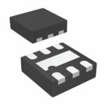 PL135-27GI-R

The activity of extra discounts on wholesale prices is in full swing…
Please fill in your contact information and we will send you the latest wholesale price list.






