ChipApex | Global Electronic Components Supplier
SEARCH
Search Product
Search Post
— IC芯片 | 连接器 | 传感器 | 被动器件 —
Search productSearch post
— IC芯片 | 连接器 | 传感器 | 被动器件 —
Consult the customer manager about the wholesale price.
consultation hotline:86-132-6715-2157
email:[email protected]
Contact the product manager for consultation. One-stop consultation is available.
Do you want a lower wholesale price? Please send us your inquiry and we will reply immediately.
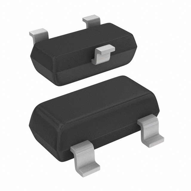
The PMBFJ177,215 is a P-channel silicon junction field-effect transistor (JFET) manufactured by NXP Semiconductors. It is housed in a plastic microminiature SOT-23 surface-mount package with three leads. The device features symmetrical construction allowing interchangeable drain and source connections. Key electrical specifications include a maximum drain-source voltage of 30 V and a gate-source breakdown voltage of 30 V. At a drain-source voltage of -15 V and zero gate-source voltage, the typical drain current is 20 mA, with a range of 1.5 to 20 mA. The typical drain-source on-resistance is 300 Ω at -0.1 V and zero gate bias.
Verify the component authenticity against the official NXP datasheet revision 3.0 dated January 24, 2020. Confirm the marking code corresponds to '6Y' prefixed by the manufacturing site identifier. Ensure the ordering suffix matches the specified tape-and-reel packaging configuration for the SOT-23 envelope.
Select this component when a low-current P-channel JFET is required for analogue signal routing or switching applications. The specific drain current and on-resistance characteristics distinguish it from other variants in the PMBFJ174 through PMBFJ177 series. Verify that the 300 Ω on-resistance aligns with the load requirements of the target circuit design.
This part belongs to the PMBFJ174/175/176/177 family of P-channel silicon field-effect transistors. All members share identical physical packages, pin configurations, and general descriptions but differ in their specific static electrical parameters, particularly drain current and on-resistance values.
Direct substitutes within the same family include PMBFJ174, PMBFJ175, and PMBFJ176. Note that these alternatives possess different drain current and resistance specifications compared to the PMBFJ177.
No, the device features a symmetrical structure where the drain and source connections are interchangeable.
The maximum gate-source breakdown voltage is rated at 30 V.
While they share the same package and general description, the PMBFJ177 has a lower typical drain current (20 mA vs 135 mA) and higher on-resistance (300 Ω vs 85 Ω).
 PMBFJ177,215
The activity of extra discounts on wholesale prices is in full swing…
Please fill in your contact information and we will send you the latest wholesale price list.