 ChipApex | Global Electronic Components Supplier
SEARCH
Search Product
Search Post
— IC芯片 | 连接器 | 传感器 | 被动器件 —
Search productSearch post
— IC芯片 | 连接器 | 传感器 | 被动器件 —
Consult the customer manager about the wholesale price.
consultation hotline:86-132-6715-2157
email:[email protected]
Contact the product manager for consultation. One-stop consultation is available.
Do you want a lower wholesale price? Please send us your inquiry and we will reply immediately.
The PMP5201G is a PNP/PNP matched double transistor housed in a SOT353 (SC-88A) TSSOP5 plastic surface-mounted package. It features a common emitter configuration with an application-optimized pinout and is qualified under AEC-Q101 standards for automotive use. Key electrical parameters include a collector-emitter voltage of -45 V, a collector current of -100 mA, and a DC current gain ranging from 200 to 450 at -5 V and -2 mA. The device exhibits tight matching characteristics, with hFE1/hFE2 ratios between 0.98 and 1.02 and base-emitter voltage differences within ±2 mV.
Verify the specific ordering suffix against official Nexperia documentation to confirm packaging details and manufacturing site codes. Confirm that the component status remains active for new designs, as product lifecycles may change. Ensure compliance with RoHS directives and automotive qualification requirements relevant to the target application environment before finalizing procurement.
Select this component when precise matching between two PNP transistors is required for analog circuits. The SOT353 package offers a compact footprint suitable for space-constrained designs. Consider the thermal resistance values and power dissipation limits relative to the operating ambient temperature and PCB copper area to ensure reliable operation within specified junction temperature ranges.
This part belongs to the PMP series of matched double transistors manufactured by Nexperia. It serves as the PNP/PNP complement to the NPN/NPN PMP4201G and has a complementary counterpart in the PMP5501G. The device replaces older variants like the PMP5201V while maintaining similar electrical performance in a standardized small outline package.
Direct functional substitutes include the PMP5201V and PMP5201Y, which share identical electrical specifications but differ in package type or suffix designation. Verify pin compatibility and package dimensions when swapping between these variants to ensure mechanical fit on the printed-circuit board.
The total power dissipation is 200 mW per transistor and 300 mW per device when the ambient temperature is less than or equal to 25 °C.
The base-emitter saturation voltage decreases by approximately 1.7 mV/K as the temperature increases.
Yes, the product has been qualified in accordance with the Automotive Electronics Council standard Q101 and is suitable for use in automotive applications.
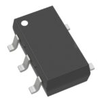 PMP5201G,115
The activity of extra discounts on wholesale prices is in full swing…
Please fill in your contact information and we will send you the latest wholesale price list.






