 ChipApex | Global Electronic Components Supplier
SEARCH
Search Product
Search Post
— IC芯片 | 连接器 | 传感器 | 被动器件 —
Search productSearch post
— IC芯片 | 连接器 | 传感器 | 被动器件 —
Consult the customer manager about the wholesale price.
consultation hotline:86-132-6715-2157
email:[email protected]
Contact the product manager for consultation. One-stop consultation is available.
Do you want a lower wholesale price? Please send us your inquiry and we will reply immediately.
The PMP5201Y,115 is a PNP/PNP matched double transistor manufactured by Nexperia in a SOT363-3 (TSSOP6) surface-mount package. It features a collector-emitter voltage of -45 V and a maximum collector current of -100 mA per transistor. The device offers a DC current gain ranging from 200 to 450 at -2 mA. Key matching specifications include a current gain ratio of 0.98 to 1.02 and a base-emitter voltage difference within ±2 mV. Total power dissipation is rated at 300 mW, with an operating temperature range from -65 °C to +150 °C.
Verify the specific ordering suffix against the manufacturer's official documentation to confirm the exact packaging configuration. Confirm that the component status remains active for new designs before finalizing procurement plans. Ensure compliance with RoHS directives as specified in the product data sheet.
Select this component when precise matching between dual PNP transistors is required for analog circuits. The SOT363-3 package provides a compact footprint suitable for space-constrained designs. Evaluate thermal resistance characteristics if operation near maximum power dissipation limits is anticipated.
This part belongs to Nexperia's portfolio of matched double transistors. It serves as the PNP/PNP complement to the NPN/NPN PMP4201Y. The device utilizes silicon technology and is designed for general-purpose switching and amplification applications requiring high matching accuracy.
The PMP5201V is a functional equivalent available in the SOT666 package. Designers must account for differences in pinout configurations and physical dimensions when substituting between these package types.
The total power dissipation for the device is 300 mW when mounted on an FR4 printed-circuit board at an ambient temperature of 25 °C or lower.
The base-emitter voltage matching (VBE1−VBE2) is specified to be within ±2 mV under conditions of VCE = -5 V, IC = -2 mA, and Tamb = 25 °C.
The maximum collector-base voltage (VCBO) with the emitter open is -50 V.
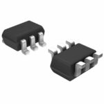 PMP5201Y,115
The activity of extra discounts on wholesale prices is in full swing…
Please fill in your contact information and we will send you the latest wholesale price list.




