 ChipApex | Global Electronic Components Supplier
SEARCH
Search Product
Search Post
— IC芯片 | 连接器 | 传感器 | 被动器件 —
Search productSearch post
— IC芯片 | 连接器 | 传感器 | 被动器件 —
Consult the customer manager about the wholesale price.
consultation hotline:86-132-6715-2157
email:[email protected]
Contact the product manager for consultation. One-stop consultation is available.
Do you want a lower wholesale price? Please send us your inquiry and we will reply immediately.
The Nexperia PMP5201Y,135 is a matched double transistor featuring two PNP transistors integrated into a SOT363-3 (TSSOP6) surface-mounted package. It provides a collector-emitter voltage of -45 V and a continuous collector current of -100 mA per transistor. The device exhibits a typical DC current gain of 290 at -2 mA and maintains tight matching characteristics with a current gain ratio of 0.98 to 1.02 and base-emitter voltage matching within ±2 mV. Total power dissipation reaches 300 mW, supporting operation across an ambient temperature range of -65 °C to +150 °C.
Verify the specific ordering suffix against official Nexperia documentation to confirm packaging details and manufacturing site codes. Ensure that the selected variant matches the required tape-and-reel specifications for automated assembly processes. Cross-reference the component marking code 'S9%' with production records to validate authenticity and traceability during the sourcing phase.
Select this component when precise matching between dual PNP transistors is required in compact designs. The SOT363-3 package offers space efficiency compared to discrete alternatives. Evaluate thermal resistance limits under actual PCB mounting conditions to ensure junction temperatures remain within safe operating areas during high-current switching or amplification tasks.
This part belongs to Nexperia's matched double transistor family, designed for applications requiring symmetrical electrical characteristics. It serves as the PNP/PNP complement to the NPN/NPN PMP4201Y series. The device utilizes silicon technology and is housed in a plastic surface-mounted package suitable for standard reflow soldering processes on FR4 printed-circuit boards.
PMP5201V,115
The total power dissipation for the entire device is 300 mW when the ambient temperature is 25 °C or lower.
The base-emitter voltage difference (VBE1−VBE2) is matched to within ±2 mV when measured at VCE = -5 V, IC = -2 mA, and Tamb = 25 °C.
The maximum collector-base voltage (VCBO) is limited to -50 V with the emitter open.
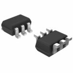 PMP5201Y,135
The activity of extra discounts on wholesale prices is in full swing…
Please fill in your contact information and we will send you the latest wholesale price list.




