 ChipApex | Global Electronic Components Supplier
SEARCH
Search Product
Search Post
— IC芯片 | 连接器 | 传感器 | 被动器件 —
Search productSearch post
— IC芯片 | 连接器 | 传感器 | 被动器件 —
Consult the customer manager about the wholesale price.
consultation hotline:86-132-6715-2157
email:[email protected]
Contact the product manager for consultation. One-stop consultation is available.
Do you want a lower wholesale price? Please send us your inquiry and we will reply immediately.
The PSD813F1A-90J is a Flash in-system programmable (ISP) peripheral for 8-bit MCUs, manufactured by STMicroelectronics. It integrates 1 Mbit of Primary Flash Memory and 256 Kbit of Secondary EEPROM, allowing concurrent read/write operations between the two arrays. The device includes 16 Kbit of SRAM and over 3,000 gates of programmable logic (DPLD and CPLD). It features 27 reconfigurable I/Os and supports a single 5 V supply voltage with standby current as low as 50 µA. The component is housed in a 52-pin PLCC package.
Verify that the design does not require new development, as this product is not recommended for new designs. Confirm compatibility with existing 8-bit MCU architectures and ensure the 52-PLCC package fits the target PCB footprint. Check for RoHS compliance status if required by specific regional regulations.
Select this component when simultaneous code execution and data logging are required using separate Flash and EEPROM banks. Ensure the application utilizes an 8-bit MCU compatible with the multiplexed or non-multiplexed bus interfaces described in the datasheet. Verify that the 5 V supply voltage aligns with the system power requirements.
This part belongs to the PSD813F1A family of Programmable Microcontroller Peripherals from STMicroelectronics. The 'J' suffix indicates the 52-pin Plastic Leaded Chip Carrier (PLCC) package variant. Other variants in the series include PQFP52 and TQFP64 packages, offering different form factors for similar functional capabilities.
Public confirmed substitute part numbers are not available in the provided documentation. Designers should consult STMicroelectronics for current alternative recommendations within the PSD family or general-purpose programmable peripherals.
Yes, it supports In-System Programming (ISP) via a standard JTAG interface, allowing the Flash memory, EEPROM, and PLD to be programmed without removing the device from the circuit.
The Primary Flash Memory has an endurance of 100,000 Erase/Write cycles, while the Secondary EEPROM supports 10,000 Erase/Write cycles.
The dual-bank architecture allows the MCU to execute code from one memory array (e.g., Flash) while simultaneously erasing and writing to the other array (e.g., EEPROM).
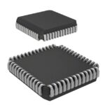 PSD813F1A-90J
The activity of extra discounts on wholesale prices is in full swing…
Please fill in your contact information and we will send you the latest wholesale price list.





