 ChipApex | Global Electronic Components Supplier
SEARCH
Search Product
Search Post
— IC芯片 | 连接器 | 传感器 | 被动器件 —
Search productSearch post
— IC芯片 | 连接器 | 传感器 | 被动器件 —
Consult the customer manager about the wholesale price.
consultation hotline:86-132-6715-2157
email:[email protected]
Contact the product manager for consultation. One-stop consultation is available.
Do you want a lower wholesale price? Please send us your inquiry and we will reply immediately.
The PSD813F2A-70J is a Flash In-System Programmable (ISP) peripheral for 8-bit microcontrollers manufactured by STMicroelectronics. It features dual-bank flash memory architecture with up to 2 Mbit of primary flash and 256 Kbit of secondary flash, supporting concurrent read/erase/write operations. The device includes 256 Kbit of battery-backed SRAM and over 3000 gates of PLD logic. It provides 27 reconfigurable I/O ports and a built-in JTAG-compliant serial port for full-chip in-system programming. Operating on a single 5V supply, it is housed in a 52-pin LCC package.
Verify the specific suffix 'J' corresponds to the 52-LCC (J-Lead) plastic package as indicated by the supplier data. Confirm the operating temperature range matches the application requirements, as standard industrial grades typically extend to 70°C. Ensure the design supports the 5V single-supply voltage requirement and utilizes the JTAG interface for programming.
Select this component when an 8-bit MCU requires significant external program memory and flexible logic resources without additional discrete components. The dual-bank flash allows for robust code protection and background updates. Consider the 52-pin package size and pin count against PCB layout constraints. Verify compatibility with the target MCU's address and data bus widths.
This part belongs to the PSD8xxxF2 series of Flash ISP peripherals from STMicroelectronics. These devices are designed to augment 8-bit microcontrollers by providing large amounts of flash memory and programmable logic in a single chip. The 'F2' designation typically indicates the dual-bank flash architecture with concurrent operation capabilities compared to earlier single-bank variants.
Direct replacements within the same family include other PSD813F2 variants with different speed grades or package options, such as the PSD813F2A-90J. Cross-family migration to newer ST programmable peripherals should be evaluated based on pin compatibility and software toolchain support.
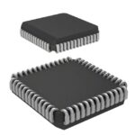 PSD813F2A-70J
The activity of extra discounts on wholesale prices is in full swing…
Please fill in your contact information and we will send you the latest wholesale price list.






