 ChipApex | Global Electronic Components Supplier

SEARCH
Search Product
Search Post
— IC芯片 | 连接器 | 传感器 | 被动器件 —
Search productSearch post
— IC芯片 | 连接器 | 传感器 | 被动器件 —
Consult the customer manager about the wholesale price.
consultation hotline:86-132-6715-2157
email:[email protected]
Contact the product manager for consultation. One-stop consultation is available.
Do you want a lower wholesale price? Please send us your inquiry and we will reply immediately.
PT7C4511WE is listed in the Clock Generators, PLLs, Frequency Synthesizers range at ChipApex. The manufacturer field lists Diodes Incorporated. Its product description is IC PLL CLOCK MULT 8-SOIC. Review the specifications below when checking this part for your BOM.
The PT7C4511WE is a PLL clock multiplier manufactured by Diodes Incorporated, designed for synthesizing and distributing high-speed clock signals. It operates on a single supply voltage ranging from 3.0V to 5.5V and supports input frequencies between 1 MHz and 50 MHz. The device generates output frequencies up to 200 MHz at 5.0V or 180 MHz at 3.3V. Clock multiplication ratios are selectable via S0 and S1 pins, offering factors of ×2, ×2.5, ×3, ×4, ×5, ×6, ×8, and fractional multipliers such as ×(10/3) and ×(16/3). The component utilizes an internal crystal oscillator or external clock input and features a tri-state output controlled by the OE pin.
Verify that the ordering suffix matches the required package and reel configuration. The 'W' designation indicates an SOIC-8 package, while the 'E' suffix confirms lead-free and green manufacturing compliance. The 'X' suffix specifies tape and reel packaging. Confirm the specific part number variant against the manufacturer's current datasheet revision to ensure compatibility with design requirements.
Select this component when a single-supply PLL clock multiplier is required for frequencies up to 200 MHz. Ensure the application voltage falls within the 3.0V to 5.5V range. Verify that the desired multiplication factor aligns with the available S0 and S1 pin configurations. Consider the operating temperature range of -40°C to +85°C for environmental suitability.
The PT7C4511 belongs to Diodes Incorporated's family of PLL clock drivers and multipliers. It shares functional similarities with other devices in the PI6C series but is distinct in its specific multiplication options and package configuration. This model is specifically engineered for applications requiring low jitter and flexible frequency generation from a single reference source.
Public confirmed substitute part numbers are not available in the provided documentation. Evaluate alternative PLL clock multipliers based on matching supply voltage, maximum output frequency, and package dimensions if substitution is necessary.
The multiplication ratio is determined by the logic states of the S0 and S1 pins. These pins can be connected to GND, Vcc, or left floating (which self-biases to Vcc/2) to select specific integer or fractional multipliers.
The OE (Output Enable) pin controls the state of the CLK output. When the OE pin is low, the clock output is tri-stated. The pin includes an internal pull-up resistor, defaulting the output to active when unconnected.
Yes, the X1/ICLK pin can accept an external clock signal directly. In this mode, the X2 pin should be left unconnected.
Explore related parts through Clock/Timing, Integrated Circuits (ICs), all product categories, ChipApex homepage.
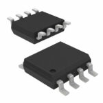 PT7C4511WE

The activity of extra discounts on wholesale prices is in full swing…
Please fill in your contact information and we will send you the latest wholesale price list.





