 ChipApex | Global Electronic Components Supplier

SEARCH
Search Product
Search Post
— IC芯片 | 连接器 | 传感器 | 被动器件 —
Search productSearch post
— IC芯片 | 连接器 | 传感器 | 被动器件 —
Consult the customer manager about the wholesale price.
consultation hotline:86-132-6715-2157
email:[email protected]
Contact the product manager for consultation. One-stop consultation is available.
Do you want a lower wholesale price? Please send us your inquiry and we will reply immediately.
The PTN3460BS/F1,518 is an embedded DisplayPort to LVDS bridge IC manufactured by NXP Semiconductors. It converts DP streams from sources like CPUs or GPUs into LVDS format for display panels. The device supports Main Link rates of 1.62 Gbit/s and 2.7 Gbit/s with 1-lane or 2-lane operation. It handles pixel clock frequencies up to 112 MHz and supports color depths of 18 bpp or 24 bpp in single or dual LVDS bus modes. Power supply options include a single 3.3 V rail or dual 3.3 V/1.8 V rails. The component is housed in a 56-terminal HVQFN package measuring 7 mm x 7 mm with a 0.4 mm pitch.
Verify the specific firmware version indicated by the suffix 'F1' against system requirements, as firmware versions are not necessarily backwards compatible. Confirm that the ordering label matches the required firmware revision. Ensure the procurement source provides documentation confirming the exact part marking and package specifications.
Select this component when interfacing eDP sources with legacy LVDS displays. Consider the F1 firmware version specifically if previous versions caused compatibility issues. Evaluate power supply constraints to determine if the internal regulator (3.3 V only) or external 1.8 V supply is preferred. Verify that the target panel resolution fits within the 112 MHz pixel clock limit.
This part belongs to the PTN3460 series of bridge ICs designed for commercial and industrial embedded applications. The 'BS' designation indicates the specific package type and temperature range, while the '/Fx' suffix denotes the firmware version programmed during manufacturing. Other variants exist with different firmware revisions or industrial temperature ratings.
Public confirmed substitute part numbers are not available in the provided documentation. Firmware-specific parts require matching firmware versions for direct replacement. Consult NXP technical support for alternative components if the current firmware version is incompatible with the host system.
The device supports EDID ROM emulation, allowing it to mimic EDID behavior for panels that lack an onboard ROM. This avoids the need for changes in the system video BIOS.
The PD_N pin is a dedicated control input for Deep power-saving state. When driven LOW, it triggers a power-down sequence. To exit this state, the pin must be driven HIGH.
Yes, the device can be powered by a single 3.3 V supply using its on-chip regulator. Alternatively, it supports dual supplies of 3.3 V and 1.8 V if the internal regulator is switched off.
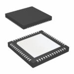 PTN3460BS/F1,518

The activity of extra discounts on wholesale prices is in full swing…
Please fill in your contact information and we will send you the latest wholesale price list.





