 ChipApex | Global Electronic Components Supplier

SEARCH
Search Product
Search Post
— IC芯片 | 连接器 | 传感器 | 被动器件 —
Search productSearch post
— IC芯片 | 连接器 | 传感器 | 被动器件 —
Consult the customer manager about the wholesale price.
consultation hotline:86-132-6715-2157
email:[email protected]
Contact the product manager for consultation. One-stop consultation is available.
Do you want a lower wholesale price? Please send us your inquiry and we will reply immediately.
The PTN3460BS is an embedded DisplayPort to LVDS bridge IC manufactured by NXP Semiconductors. It converts DP streams from CPU/GPU sources into LVDS format for display panels. The device supports link rates of 1.62 Gbit/s and 2.7 Gbit/s with 1-lane or 2-lane operation. It handles pixel clock frequencies up to 112 MHz, supporting single or dual bus LVDS signaling with 18-bit or 24-bit color depths. Power supplies include 3.3 V (±10%) and 1.8 V (±5%). Operating temperature ranges from -40 °C to +85 °C. The component is housed in a 56-terminal HVQFN package measuring 7 mm x 7 mm.
Verify the specific firmware version suffix required for the application, as versions are not necessarily backwards compatible. Confirm power supply configuration options, specifically whether the internal regulator will be used or if dual supplies are needed. Ensure the PCB layout accommodates the exposed center pad for thermal relief and electrical grounding.
Select based on the required link rate and lane count compatibility with the source GPU or CPU. Evaluate the need for EDID emulation features if the target panel lacks non-volatile memory. Consider the operating temperature range requirements for the specific deployment environment. Verify that the host system supports the necessary I2C-bus or AUX interface protocols for configuration.
The PTN3460 series serves as a bridge between Embedded DisplayPort sources and LVDS displays. It replaces discrete translation components by integrating protocol conversion, equalization, and control logic into a single chip. This integration reduces board space and simplifies design complexity for portable computing devices requiring high-resolution displays.
PTN3460IBS/F1MP is a documented industrial-grade variant within the same family. Verify pinout and firmware compatibility before substitution. Other models in the PTN3460 series may differ in firmware or environmental ratings.
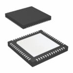 PTN3460BS,518

The activity of extra discounts on wholesale prices is in full swing…
Please fill in your contact information and we will send you the latest wholesale price list.






