 ChipApex | Global Electronic Components Supplier
SEARCH
Search Product
Search Post
— IC芯片 | 连接器 | 传感器 | 被动器件 —
Search productSearch post
— IC芯片 | 连接器 | 传感器 | 被动器件 —
Consult the customer manager about the wholesale price.
consultation hotline:86-132-6715-2157
email:[email protected]
Contact the product manager for consultation. One-stop consultation is available.
Do you want a lower wholesale price? Please send us your inquiry and we will reply immediately.
The Nexperia PUMH9 is a dual NPN Resistor-Equipped Transistor (RET) housed in a SOT363-3 (SC-88) surface-mount package. It integrates two NPN transistors with built-in bias resistors, specifically R1 = 10 kΩ and R2 = 47 kΩ. The device supports a maximum collector-emitter voltage of 50 V and an output current of 100 mA per transistor. Total power dissipation is rated at 300 mW for the device and 200 mW per transistor at 25 °C ambient temperature. Key electrical characteristics include a DC current gain (hFE) of 100 at 5 mA and a transition frequency (fT) of 230 MHz.
Verify the specific ordering suffix against the manufacturer's latest documentation to ensure correct packaging configuration. Confirm that the selected variant matches the required tape-and-reel or cut-tape specifications for automated assembly processes. Cross-reference the marking code 'H%9' with manufacturing site codes to validate authenticity and traceability during incoming inspection.
Select this component when space constraints require a dual-transistor solution with integrated biasing in a compact SOT363-3 footprint. Ensure the application voltage does not exceed the 50 V collector-emitter rating. Verify that the required input impedance aligns with the specified 10 kΩ base resistor value. Consider thermal derating curves if operating above 25 °C ambient temperature to maintain reliability within the 150 °C junction limit.
The PUMH9 belongs to Nexperia's family of Resistor-Equipped Transistors designed to replace multiple discrete components. It serves as the NPN/NPN complement to the PUMB9 (PNP/PNP) and PUMD9 (NPN/PNP). This integration reduces printed circuit board area and pick-and-place costs compared to using separate transistors and resistors.
Direct functional equivalents include the PIMH9 for general-purpose isolation needs without integrated resistors. For complementary polarity requirements, consider the PUMB9 or PUMD9 variants. Verify pinout compatibility and thermal resistance values when substituting into existing designs.
The device features a base resistor (R1) of 10 kΩ and a ratio resistor (R2) of 47 kΩ, resulting in an R2/R1 ratio of approximately 4.7.
Pin 1 is GND1 (emitter), Pin 2 is I1 (input/base), Pin 3 is O2 (collector), Pin 4 is GND2 (emitter), Pin 5 is I2 (input/base), and Pin 6 is O1 (collector).
The total power dissipation is 300 mW for the entire device and 200 mW per individual transistor when mounted on an FR4 PCB at 25 °C ambient temperature.
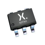 PUMH9,135
The activity of extra discounts on wholesale prices is in full swing…
Please fill in your contact information and we will send you the latest wholesale price list.




