 ChipApex | Global Electronic Components Supplier

SEARCH
Search Product
Search Post
— IC芯片 | 连接器 | 传感器 | 被动器件 —
Search productSearch post
— IC芯片 | 连接器 | 传感器 | 被动器件 —
Consult the customer manager about the wholesale price.
consultation hotline:86-132-6715-2157
email:[email protected]
Contact the product manager for consultation. One-stop consultation is available.
Do you want a lower wholesale price? Please send us your inquiry and we will reply immediately.
The PX1011BI-EL1/G,551 is a single-lane PCI Express electrical PHY compliant with Base Specification Rev. 1.0a and 1.1. It operates at 2.5 Gbit/s using an 8-bit PXPIPE interface running at 250 MHz with SSTL_2 signaling. The device supports industrial temperature range (-40°C to +85°C) and dissipates less than 300 mW in L0 mode. It requires three digital supply voltages: 3.3 V for JTAG I/O, 2.5 V for SSTL_2 I/O, and 1.2 V for the core. The package is LFBGA81 (9x9 mm).
Verify the ordering suffix 'G' indicates lead-free packaging and 'I' confirms the industrial temperature grade. Confirm the specific tape-and-reel quantity associated with the ',551' suffix if required by your assembly process. Ensure the component matches the LFBGA81 footprint dimensions of 9 x 9 mm.
Select this component when a standalone PCIe PHY is needed for FPGA integration rather than an integrated MAC solution. Ensure the design accommodates the separate voltage domains (1.2V, 2.5V, 3.3V) and the requirement for a 100 MHz external reference clock. Verify that the host system supports the PXPIPE interface protocol.
This part belongs to the NXP PX1011B family of standalone PCIe PHYs. The 'I' suffix specifically denotes the industrial temperature variant (-40°C to +85°C), distinguishing it from the commercial version (0°C to +70°C). The 'G' suffix indicates lead-free solder composition.
The PX1011B-EL1/N is the leaded equivalent. The PX1011B-EL1/Q900 is the automotive AEC-Q100 compliant version. Direct functional replacement within the same package is limited to these variants.
The device dissipates less than 300 mW in the L0 normal operational state.
PXPIPE adds source synchronous clocks for transmit and receive data to simplify timing closure for off-chip applications.
A 100 MHz external reference clock with ±300 ppm tolerance is required.
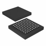 PX1011BI-EL1/G,551

The activity of extra discounts on wholesale prices is in full swing…
Please fill in your contact information and we will send you the latest wholesale price list.







