 ChipApex | Global Electronic Components Supplier
SEARCH
Search Product
Search Post
— IC芯片 | 连接器 | 传感器 | 被动器件 —
Search productSearch post
— IC芯片 | 连接器 | 传感器 | 被动器件 —
Consult the customer manager about the wholesale price.
consultation hotline:86-132-6715-2157
email:[email protected]
Contact the product manager for consultation. One-stop consultation is available.
Do you want a lower wholesale price? Please send us your inquiry and we will reply immediately.
The Nexperia PZU5.1DB2,115 is a dual isolated general-purpose Zener diode housed in the SOT353 (SC-88A) surface-mounted package. It features a nominal working voltage of 5.1 V with a tolerance of approximately ±2%. The device supports a total power dissipation of up to 250 mW and a non-repetitive peak reverse power dissipation of 40 W. Key electrical characteristics include a differential resistance of 60 Ω at IZ = 5 mA, a maximum reverse current of 2 μA, and a temperature coefficient of 0.3 mV/K. It is qualified according to AEC-Q101 standards.
Verify the specific ordering suffix against the manufacturer's current catalog to ensure correct packaging and marking codes. Confirm that the component meets the required AEC-Q101 automotive qualification standards for the intended application environment. Cross-reference the datasheet revision history to ensure the latest thermal and electrical specifications are applied during design integration.
Select this component when space-constrained designs require dual independent Zener regulators in a minimal footprint. The ±2% tolerance makes it suitable for precision applications compared to standard ±5% variants. Ensure the operating junction temperature remains within the specified -55 °C to +150 °C range to maintain performance reliability under varying thermal conditions.
This part belongs to the PZUxDB2 series, which offers a wide working voltage range from 2.7 V to 24 V. The series utilizes the SOT353 package to provide a small standard plastic solution for surface-mounted designs. It serves as a compact alternative to through-hole or larger SMD packages for high-density circuit layouts requiring dual regulation capabilities.
Direct substitutes within the same series include other PZUxDB2 types with different voltage ratings but identical pinouts and package dimensions. Verify compatibility by checking the specific Zener voltage requirements and ensuring the replacement maintains the ±2% tolerance and AEC-Q101 qualification if automotive use is required.
Pin 1 is the anode for diode 1, Pin 3 is the anode for diode 2, Pin 4 is the cathode for diode 2, Pin 5 is the cathode for diode 1, and Pin 2 is not connected.
Yes, the device is qualified according to the AEC-Q101 standard for stress test qualification of discrete semiconductors.
The maximum non-repetitive peak reverse power dissipation (PZSM) is 40 W.
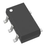 PZU5.1DB2,115
The activity of extra discounts on wholesale prices is in full swing…
Please fill in your contact information and we will send you the latest wholesale price list.




