 ChipApex | Global Electronic Components Supplier
SEARCH
Search Product
Search Post
— IC芯片 | 连接器 | 传感器 | 被动器件 —
Search productSearch post
— IC芯片 | 连接器 | 传感器 | 被动器件 —
Consult the customer manager about the wholesale price.
consultation hotline:86-132-6715-2157
email:[email protected]
Contact the product manager for consultation. One-stop consultation is available.
Do you want a lower wholesale price? Please send us your inquiry and we will reply immediately.
The QS4A205QG8 is a multiplexer/demultiplexer IC from the Renesas QS4A205 series, featuring four SPDT switch circuits configured as two 2:1 MUX-DEMUX channels. It operates within a single 5V supply voltage range of 4.75 V to 5.25 V. The device provides an on-resistance maximum of 17 Ohms and supports a -3dB bandwidth of 830 MHz. Switching times are limited to 6 ns for both turn-on and turn-off durations. It is housed in a 16-QSOP surface-mount package and functions reliably across an industrial temperature range of -40°C to +85°C.
Verify the specific suffix 'Q8' against official Renesas documentation to confirm tape-and-reel packaging versus tube configuration. Ensure the component meets RoHS3 compliance requirements for your manufacturing process. Cross-reference the manufacturer part number IDTQS4A205QG8 for accurate sourcing history and availability status.
Select this component when a 2:1 multiplexer configuration is required rather than a standard 4:1 layout. The 16-QSOP package offers a balance between pin count and board space. Consider the 17 Ohm on-resistance limit for signal integrity requirements in low-voltage analog paths.
This part belongs to the QS4A205 family of analog switches manufactured by Renesas Electronics Corporation. The family includes variants such as the QS4A205 and QS4A105, which differ in channel count and package options. The QS4A205 specifically focuses on providing dual 2:1 multiplexing functionality within a single chip.
Publicly listed substitutes include ADG774BRQZ from Analog Devices and FSAL200MTCX from onsemi. Verify pin compatibility and electrical specifications before substitution.
The device is designed to operate with a single power supply voltage ranging from 4.75 V to 5.25 V.
No, the QS4A205QG8 consists of single-ended SPDT switches and does not natively support differential signaling configurations.
The typical off-state isolation is specified at -60 dB, ensuring effective signal blocking when the switch is open.
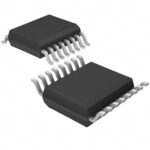 QS4A205QG8
The activity of extra discounts on wholesale prices is in full swing…
Please fill in your contact information and we will send you the latest wholesale price list.





