 ChipApex | Global Electronic Components Supplier
SEARCH
Search Product
Search Post
— IC芯片 | 连接器 | 传感器 | 被动器件 —
Search productSearch post
— IC芯片 | 连接器 | 传感器 | 被动器件 —
Consult the customer manager about the wholesale price.
consultation hotline:86-132-6715-2157
email:[email protected]
Contact the product manager for consultation. One-stop consultation is available.
Do you want a lower wholesale price? Please send us your inquiry and we will reply immediately.
The RC19008A100GND#KB0 is an eight-output PCIe Gen7 clock buffer manufactured by Renesas Electronics. It operates within a supply voltage range of 3 V to 3.6 V and supports input frequencies up to 400 MHz. The device features LP-HCSL outputs with selectable 100 Ω output impedance, eliminating the need for external termination resistors. Key electrical specifications include a maximum propagation delay of 1.8 ns and an additive phase jitter of 30 fs RMS. It functions in temperatures from -40°C to +105°C and is housed in a 5 mm × 5 mm 40-VFQFPN package.
Verify the specific ordering suffix #KB0 against official Renesas documentation to confirm pinout and packaging details, as suffixes can indicate variations in reel type or moisture sensitivity levels. Ensure the component meets RoHS requirements for the target assembly process. Cross-reference the manufacturer part number with distributor catalogs to confirm current availability status and long-term supply commitments.
Select this component when designing high-speed PCIe interfaces requiring low jitter and flexible output drive capabilities. The 100 Ω impedance version is suitable for applications needing integrated termination. Consider the 40-VFQFPN package dimensions for PCB layout constraints. Verify that the input signal source matches the supported LVDS or HCSL input types for optimal performance.
This part belongs to the RC19008 family of PCIe Gen7 clock buffers. It shares core architectural features with other variants like the RC19008A100GND#BB0 but may differ in packaging or shipping configuration based on the suffix. The family is designed to support next-generation server and communication infrastructure requirements.
The RC19008A100GND#BB0 is a related variant within the same product family. Verify if the #BB0 suffix offers identical electrical characteristics and pin compatibility before substitution. No other public substitute part numbers are confirmed.
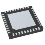 RC19008A100GND#KB0
The activity of extra discounts on wholesale prices is in full swing…
Please fill in your contact information and we will send you the latest wholesale price list.





