 ChipApex | Global Electronic Components Supplier
SEARCH
Search Product
Search Post
— IC芯片 | 连接器 | 传感器 | 被动器件 —
Search productSearch post
— IC芯片 | 连接器 | 传感器 | 被动器件 —
Consult the customer manager about the wholesale price.
consultation hotline:86-132-6715-2157
email:[email protected]
Contact the product manager for consultation. One-stop consultation is available.
Do you want a lower wholesale price? Please send us your inquiry and we will reply immediately.
The RC19016A100GN1#KB0 is a PCIe Gen7 clock buffer manufactured by Renesas Electronics. It features one differential input and sixteen differential LP-HCSL outputs, supporting frequencies up to 400 MHz. The device operates on a supply voltage of 2.97V to 3.63V and functions within an ambient temperature range of -40°C to 105°C. Packaged in a 64-VFQFPN (9x9 mm) case with an exposed pad, it is designed for high-speed serial applications requiring low jitter and robust signal integrity.
Verify the specific ordering suffix #KB0 against the manufacturer's official documentation to confirm package type and moisture sensitivity level. Ensure compliance with RoHS directives and check for any recent Product Change Notifications that may affect assembly parameters or material composition prior to procurement.
Select this component when designing systems requiring a single input to drive sixteen downstream loads with minimal additive jitter. Confirm that the target PCB layout supports the 64-VFQFPN package dimensions and thermal requirements. Verify that the system power supply remains stable within the 2.97V to 3.63V range during all operating conditions.
This part belongs to the RC190xxA family of PCIe Gen7 clock buffers. It shares functional similarities with other members like the RC19008 and RC19020 but differs in output count and package configuration. The 'A' suffix typically denotes specific impedance or performance variations within the series.
Direct pin-compatible replacements within the same family include the RC19016AGN6#BD0. For different output counts, consider the RC19008 (8-output) or RC19020 (20-output), though package and pinout differences require schematic review.
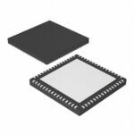 RC19016A100GN1#KB0
The activity of extra discounts on wholesale prices is in full swing…
Please fill in your contact information and we will send you the latest wholesale price list.




