 ChipApex | Global Electronic Components Supplier
SEARCH
Search Product
Search Post
— IC芯片 | 连接器 | 传感器 | 被动器件 —
Search productSearch post
— IC芯片 | 连接器 | 传感器 | 被动器件 —
Consult the customer manager about the wholesale price.
consultation hotline:86-132-6715-2157
email:[email protected]
Contact the product manager for consultation. One-stop consultation is available.
Do you want a lower wholesale price? Please send us your inquiry and we will reply immediately.
The RC19016AGN1#BB0 is a PCIe Gen7 compliant clock buffer manufactured by Renesas Electronics. It features one differential input and sixteen LP-HCSL differential outputs, providing a 1:16 fanout ratio. The device supports input frequencies up to 400 MHz with a maximum propagation delay of 1.8 ns. It operates on a single 3.3 V supply (2.97V to 3.63V) within an industrial temperature range of -40°C to +105°C. Packaged in a 64-pin VFQFPN (9x9 mm), it includes 85 Ω output impedance and SMBus control capabilities.
Verify the specific ordering suffix #BB0 against the manufacturer's current datasheet to confirm package type and moisture sensitivity level. Ensure the design accounts for the 64-VFQFPN exposed pad thermal requirements and the 3.3 V power supply tolerance limits specified in the official documentation.
Select this component when a 16-channel fanout buffer is required for PCIe Gen7 applications. It is suitable for designs needing LP-HCSL signaling to reduce termination resistor count. Compare against other RC190xxA variants if different output counts or impedance options are needed.
This part belongs to the RC190xxA family of PCIe Gen7 clock buffers. It shares architectural similarities with models like the RC19008 and RC19020 but provides a specific 16-output configuration. The family is designed for robust clock distribution in high-speed serial interfaces.
Direct pin-compatible replacements within the same family include the RC19016AGN1#BD0. Verify functional equivalence and package dimensions before substitution.
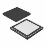 RC19016AGN1#BB0
The activity of extra discounts on wholesale prices is in full swing…
Please fill in your contact information and we will send you the latest wholesale price list.






