 ChipApex | Global Electronic Components Supplier
SEARCH
Search Product
Search Post
— IC芯片 | 连接器 | 传感器 | 被动器件 —
Search productSearch post
— IC芯片 | 连接器 | 传感器 | 被动器件 —
Consult the customer manager about the wholesale price.
consultation hotline:86-132-6715-2157
email:[email protected]
Contact the product manager for consultation. One-stop consultation is available.
Do you want a lower wholesale price? Please send us your inquiry and we will reply immediately.
The RC19016AGN1#KB0 is a PCIe Gen7 clock buffer manufactured by Renesas Electronics. It features one differential input and sixteen LP-HCSL differential outputs, providing a 1:16 fanout ratio. The device supports input frequencies up to 400 MHz with supply voltages ranging from 2.97V to 3.63V. It operates within an ambient temperature range of -40°C to +105°C and is housed in a 64-VFQFPN package measuring 9x9 mm.
Verify the specific ordering suffix #KB0 against official documentation to confirm packaging details, as suffixes often denote reel versus tray configurations. Ensure the component meets RoHS requirements and check moisture sensitivity levels prior to surface mount assembly processes.
Select this component when a single differential input must drive sixteen LP-HCSL loads with minimal jitter degradation. Confirm that the system requires 85Ω output impedance and operates within the specified 2.97V to 3.63V voltage range. Verify thermal management capabilities for the 64-VFQFPN package under maximum load conditions.
This part belongs to the RC190xxA family of PCIe Gen7 clock buffers. It shares architectural similarities with other members like the RC19008 and RC19020 but offers a specific 16-output configuration. The series is designed to reduce terminated resistors and simplify board layout for high-speed serial interfaces.
Direct pin-compatible replacements within the same family include the RC19016AGN1#BD0. Other output count variants such as the RC19008 (8-output) or RC19020 (20-output) may require schematic modifications.
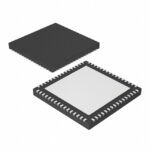 RC19016AGN1#KB0
The activity of extra discounts on wholesale prices is in full swing…
Please fill in your contact information and we will send you the latest wholesale price list.





