 ChipApex | Global Electronic Components Supplier
SEARCH
Search Product
Search Post
— IC芯片 | 连接器 | 传感器 | 被动器件 —
Search productSearch post
— IC芯片 | 连接器 | 传感器 | 被动器件 —
Consult the customer manager about the wholesale price.
consultation hotline:86-132-6715-2157
email:[email protected]
Contact the product manager for consultation. One-stop consultation is available.
Do you want a lower wholesale price? Please send us your inquiry and we will reply immediately.
The RC19020A072GN2#BB0 is a PCIe Gen7 compliant clock buffer manufactured by Renesas Electronics. It features one differential input and twenty LP-HCSL outputs, supporting frequencies up to 400 MHz. The device operates on a single 3.3 V supply (2.97V ~ 3.63V) within an industrial temperature range of -40°C to +105°C. Packaged in a 72-VFQFPN (10x10 mm) with an exposed pad, it provides ultra-low additive jitter and reduced in-to-out delay for robust signal integrity.
Verify the specific ordering suffix #BB0 against official documentation to confirm tape-and-reel packaging and moisture sensitivity level requirements. Confirm RoHS compliance status and lead-free specifications prior to procurement to ensure adherence to environmental regulations and assembly processes.
Select this component when designing systems requiring 20-channel fanout for PCIe Gen7 interfaces. Ensure the design supports LP-HCSL signaling standards and accommodates the 72-VFQFPN package dimensions. Verify that the power supply voltage remains within the 2.97V to 3.63V range for optimal performance.
This part belongs to the RC190xxA family of high-performance clock buffers designed for next-generation PCIe applications. It serves as a direct replacement for legacy components like the DB2000Q while adding Loss-Of-Signal (LOS) indication and Side-Band Interface (SBI) capabilities for enhanced system monitoring and control.
The RC19020A072GN2#BB0 is pin-compatible with the DB2000Q/DB2000QL plus additional LOS and SBI_OUT pins. Verify board layout compatibility when replacing older buffers, ensuring connections for the extra control pins are properly handled or left unconnected if unused.
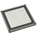 RC19020A072GN2#BB0
The activity of extra discounts on wholesale prices is in full swing…
Please fill in your contact information and we will send you the latest wholesale price list.






