 ChipApex | Global Electronic Components Supplier
SEARCH
Search Product
Search Post
— IC芯片 | 连接器 | 传感器 | 被动器件 —
Search productSearch post
— IC芯片 | 连接器 | 传感器 | 被动器件 —
Consult the customer manager about the wholesale price.
consultation hotline:86-132-6715-2157
email:[email protected]
Contact the product manager for consultation. One-stop consultation is available.
Do you want a lower wholesale price? Please send us your inquiry and we will reply immediately.
The RC19020A072GN2#KB0 is a PCIe Gen7 compliant clock buffer manufactured by Renesas Electronics. It features one differential input and twenty LP-HCSL outputs, supporting frequencies up to 400 MHz. The device operates on a single 3.3V supply (2.97V to 3.63V) within an industrial temperature range of -40°C to +105°C. Packaged in a 72-VFQFPN (10x10 mm) case, it provides ultra-low additive jitter and reduced in-to-out delay performance. Key functional attributes include power down tolerance, flexible startup sequencing, automatic clock parking, and open-drain loss-of-signal indication.
Verify the specific ordering suffix #KB0 against official Renesas documentation to confirm package type and tape-and-reel specifications. Ensure the selected variant matches the required 72-VFQFPN footprint and moisture sensitivity level for the intended manufacturing process.
Select this component when designing for PCIe Gen7 standards requiring high fan-out ratios. Confirm that the system power budget accommodates the typical power consumption and that the 3.3V core voltage aligns with the platform's power rails. Verify thermal requirements for the 10x10mm package under maximum operating conditions.
This part belongs to the RC190xxA family of clock buffers designed for high-speed serial interfaces. It serves as a direct replacement or upgrade path for legacy devices like the DB2000Q, offering enhanced signal integrity features and additional control pins such as SBI_OUT for daisy-chaining multiple clock generators.
The RC19020A072 is pin-compatible with the DB2000Q/DB2000QL plus variants. Designers migrating from these older components should verify that the new LOS indication and SMBus features are correctly integrated into the existing board layout.
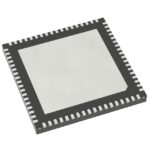 RC19020A072GN2#KB0
The activity of extra discounts on wholesale prices is in full swing…
Please fill in your contact information and we will send you the latest wholesale price list.






