ChipApex | Global Electronic Components Supplier
SEARCH
Search Product
Search Post
— IC芯片 | 连接器 | 传感器 | 被动器件 —
Search productSearch post
— IC芯片 | 连接器 | 传感器 | 被动器件 —
Consult the customer manager about the wholesale price.
consultation hotline:86-132-6715-2157
email:[email protected]
Contact the product manager for consultation. One-stop consultation is available.
Do you want a lower wholesale price? Please send us your inquiry and we will reply immediately.
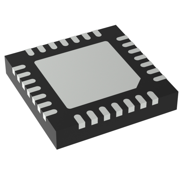
The RC19104A001GNL#BB0 is a Renesas Electronics clock buffer designed for PCIe Gen7 applications. It operates on a single 1.8V supply and provides four differential outputs. The device features ultra-low additive phase jitter, specified at 2.6fs RMS for PCIe Gen7 compliance. It supports flexible start-up timing, automatic clock holdover upon loss of the input clock, and spread-spectrum tolerance. The component accepts HCSL or LVDS input signals and offers selectable differential output impedances of 33Ω, 85Ω, or 100Ω via pin or SMBus configuration.
Verify the specific ordering suffix against the manufacturer's official documentation to confirm package type and tape/reel specifications. Confirm RoHS compliance status through the relevant environmental files provided by Renesas Electronics. Ensure the selected variant matches the required output impedance settings for the target PCB design.
Select this component when designing for PCIe Gen7 standards requiring minimal added jitter. Verify that the 1.8V supply voltage aligns with the system power architecture. Check if the 28-VFQFPN package dimensions fit the available board space. Confirm compatibility with HCSL or LVDS source drivers before finalizing the design.
This part belongs to the RC191xx series of 1.8V PCIe Gen7 buffers. It serves as a fanout buffer to distribute reference clocks to multiple downstream components. The series is characterized by backward compatibility with earlier PCIe generations while optimizing performance for next-generation high-speed serial links.
Publicly confirmed substitute part numbers are not available in the provided data. Consult Renesas Electronics for current cross-reference information.
 RC19104A001GNL#BB0
The activity of extra discounts on wholesale prices is in full swing…
Please fill in your contact information and we will send you the latest wholesale price list.