 ChipApex | Global Electronic Components Supplier
SEARCH
Search Product
Search Post
— IC芯片 | 连接器 | 传感器 | 被动器件 —
Search productSearch post
— IC芯片 | 连接器 | 传感器 | 被动器件 —
Consult the customer manager about the wholesale price.
consultation hotline:86-132-6715-2157
email:[email protected]
Contact the product manager for consultation. One-stop consultation is available.
Do you want a lower wholesale price? Please send us your inquiry and we will reply immediately.
The RC19204AGNL#BB0 is a PCIe Gen7 clock multiplexer manufactured by Renesas Electronics. It provides a 2:4 input-to-output ratio with differential LVDS or HCSL inputs and LP-HCSL outputs. The device supports frequencies up to 400MHz and operates on a single supply voltage ranging from 2.97V to 3.63V. Designed for high-performance timing applications, it features ultra-low additive jitter and reduced in-to-out delay performance. The component is housed in a 28-VFQFPN package (4x4mm) with an exposed pad, suitable for surface mount assembly across an operating temperature range of -40°C to +105°C.
Verify the specific ordering suffix #BB0 against official Renesas documentation to confirm tape-and-reel packaging details. Confirm moisture sensitivity level and reflow soldering profiles prior to procurement. Ensure compatibility with existing board designs regarding the 28-VFQFPN footprint and thermal requirements.
Select this component for designs requiring a 2:4 PCIe clock multiplexing solution with low jitter characteristics. Ensure the input signal matches the supported LVDS or HCSL standards. Verify that the system power supply remains within the 2.97V to 3.63V range. Consider the 4x4mm package size for space-constrained PCB layouts.
This part belongs to the RC19204 series of PCIe clock multiplexers. It serves as a critical timing element in modern server architectures, specifically designed to support advanced interconnect standards like PCIe Gen7. The device integrates multiple features to simplify design implementation while maintaining signal integrity.
Public confirmed substitute part numbers are not available in the provided source material.
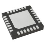 RC19204AGNL#BB0
The activity of extra discounts on wholesale prices is in full swing…
Please fill in your contact information and we will send you the latest wholesale price list.






