 ChipApex | Global Electronic Components Supplier
SEARCH
Search Product
Search Post
— IC芯片 | 连接器 | 传感器 | 被动器件 —
Search productSearch post
— IC芯片 | 连接器 | 传感器 | 被动器件 —
Consult the customer manager about the wholesale price.
consultation hotline:86-132-6715-2157
email:[email protected]
Contact the product manager for consultation. One-stop consultation is available.
Do you want a lower wholesale price? Please send us your inquiry and we will reply immediately.
The RC19216AGN6#BD0 is a PCIe Gen7 2:16 clock multiplexer from Renesas Electronics, designed for backward compatibility with earlier PCIe generations. It features LP-HCSL outputs that eliminate up to 64 terminated resistors and supports selectable 85Ω or 100Ω output impedance. The device operates on a 3.3V supply (2.97V–3.63V) within a -40°C to 105°C temperature range. Key electrical parameters include a typical additive phase jitter of 37 fs RMS and a noise floor of -154 dBc/Hz. Packaged in a 6mm × 6mm 80-GQFN, it integrates SMBus control, LOS indication, and flexible startup sequencing.
Verify the specific suffix BD0 against official datasheets to confirm package dimensions and lead finish specifications. Ensure the design supports the required 3.3V core voltage and thermal dissipation for the 80-GQFN package. Confirm that the selected address configuration aligns with system SMBus topology requirements.
Select this component when a single source must drive multiple downstream PCIe endpoints with low jitter. Compare against the RC19202 (2:2) or RC19308 (2:8) if fewer outputs are sufficient. Verify input signal compatibility with LVDS or HCSL sources and ensure the PCB layout accommodates the 6mm x 6mm footprint.
This part belongs to the RC19216A series of PCIe clock multiplexers. It serves as a high-fanout solution for distributing reference clocks in complex server architectures. It complements other Renesas timing devices like the RC190xxA buffer series for comprehensive clock tree management.
Direct pin-compatible replacements within the same family may include variants with different suffixes indicating packaging or tape-and-reel options. Cross-family substitution requires careful evaluation of I/O voltage levels and pin assignments.
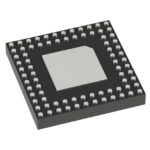 RC19216AGN6#BD0
The activity of extra discounts on wholesale prices is in full swing…
Please fill in your contact information and we will send you the latest wholesale price list.





