 ChipApex | Global Electronic Components Supplier
SEARCH
Search Product
Search Post
— IC芯片 | 连接器 | 传感器 | 被动器件 —
Search productSearch post
— IC芯片 | 连接器 | 传感器 | 被动器件 —
Consult the customer manager about the wholesale price.
consultation hotline:86-132-6715-2157
email:[email protected]
Contact the product manager for consultation. One-stop consultation is available.
Do you want a lower wholesale price? Please send us your inquiry and we will reply immediately.
The REF194GP is a precision micropower low dropout voltage reference from the Analog Devices REF19x series. It provides a nominal output voltage of 4.50 V with an initial accuracy of ±2 mV maximum at 25°C. The device features a temperature coefficient of 5 ppm/°C maximum and operates over an extended industrial temperature range of −40°C to +85°C. It delivers a high output current of 30 mA while consuming a maximum supply current of 45 μA. A sleep mode reduces supply current to 15 μA maximum. The unit includes short-circuit protection and is available in an 8-lead SOIC package.
Verify the specific electrical grade (E or G) required for your application, as line and load regulation specifications vary between grades. Confirm the package suffix matches the desired form factor, such as SOIC or PDIP. Ensure the ordering part number aligns with the required initial accuracy and temperature coefficient limits defined in the datasheet tables.
Select the REF194GP when a stable 4.50 V reference is needed with low power consumption. Consider the E grade for tighter line and load regulation specifications compared to the G grade. Evaluate the dropout voltage requirements against the input supply voltage to ensure proper operation within the specified load current range.
The REF194 is part of the broader REF19x series of precision band gap voltage references. This family includes variants with different nominal output voltages, such as 2.048 V, 2.50 V, 3.00 V, and 5.00 V. All members share common architectural features like micropower operation, low dropout characteristics, and a sleep mode function.
Direct replacements within the same series include other REF19x variants if the output voltage requirement differs. For identical 4.50 V performance, verify that alternative components match the 30 mA output current capability and the 5 ppm/°C temperature coefficient specification.
Test Pins 1 and 5 are reserved for in-package Zener zap trimming used by the factory to achieve high accuracy. Users should leave these pins unconnected.
Sleep mode is enabled by applying a low TTL or CMOS level to the SLEEP pin. This turns off the output and reduces the supply current to less than 15 μA.
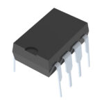 REF194GP
The activity of extra discounts on wholesale prices is in full swing…
Please fill in your contact information and we will send you the latest wholesale price list.






