ChipApex | Global Electronic Components Supplier
SEARCH
Search Product
Search Post
— IC芯片 | 连接器 | 传感器 | 被动器件 —
Search productSearch post
— IC芯片 | 连接器 | 传感器 | 被动器件 —
Consult the customer manager about the wholesale price.
consultation hotline:86-132-6715-2157
email:[email protected]
Contact the product manager for consultation. One-stop consultation is available.
Do you want a lower wholesale price? Please send us your inquiry and we will reply immediately.
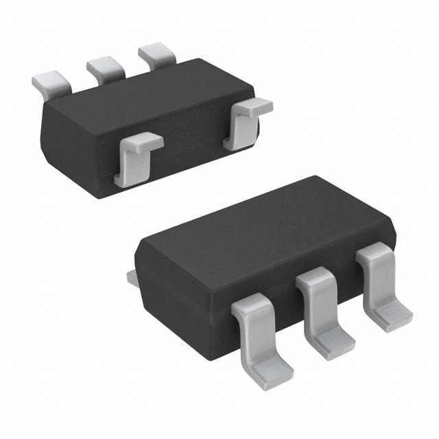
The REF2025QDDCRQ1 is an automotive-grade dual-output voltage reference featuring a 2.5 V VREF output and a 1.25 V VBIAS (VREF/2) output. It operates within a supply voltage range of VREF + 0.02 V to 5.5 V, consuming a maximum quiescent current of 460 µA across the -40°C to +125°C temperature range. The device provides high initial accuracy of ±0.05% and low temperature drift of 8 ppm/°C. Both outputs support ±20 mA load currents with a dropout voltage as low as 10 mV.
Verify that the specific suffix QDDCRQ1 corresponds to the AEC-Q100 qualified automotive grade variant with the SOT-23-5 package. Confirm functional safety documentation availability if required for system design. Ensure the ordering code matches the exact voltage configuration and packaging requirements for the target application.
Select this component when a stable mid-rail bias voltage is required alongside a primary reference in single-supply ADC circuits. The integrated VBIAS output eliminates the need for external resistor dividers, reducing board space and cost. Consider the low dropout characteristic for battery-operated systems where input voltage may approach the output level.
This part belongs to the REF20xx-Q1 family of low-drift, low-power dual-output voltage references. The family includes variants with different nominal output voltages, such as 3.0 V, 3.3 V, and 4.096 V, all sharing the same dual-output topology and performance characteristics. The Q1 designation indicates automotive qualification.
Other members of the REF20xx-Q1 family, such as REF2030QDDCRQ1 or REF2033QDDCRQ1, offer identical pinouts and features but with different fixed output voltages.
 REF2025QDDCRQ1
The activity of extra discounts on wholesale prices is in full swing…
Please fill in your contact information and we will send you the latest wholesale price list.