ChipApex | Global Electronic Components Supplier
SEARCH
Search Product
Search Post
— IC芯片 | 连接器 | 传感器 | 被动器件 —
Search productSearch post
— IC芯片 | 连接器 | 传感器 | 被动器件 —
Consult the customer manager about the wholesale price.
consultation hotline:86-132-6715-2157
email:[email protected]
Contact the product manager for consultation. One-stop consultation is available.
Do you want a lower wholesale price? Please send us your inquiry and we will reply immediately.
The S-19630AB0A-K8T2U is a dual zero-drift CMOS operational amplifier designed for automotive applications with operation up to 125°C. It utilizes chopper-stabilizing techniques to achieve low input offset voltage of +50 μV max and drift of ±25 nV/°C typ across the temperature range. The device operates on a supply voltage of 4.0 V to 36.0 V, consuming 250 μA per circuit. Key electrical parameters include a gain-bandwidth product of 1.2 MHz, slew rate of 0.45 V/μs, and rail-to-rail input/output capability. It features built-in output current limiting and internal phase compensation.
Verify AEC-Q100 qualification status directly with sales representatives as details are not publicly listed. Confirm that vehicle equipment usage requires prior contact with the manufacturer. Ensure ordering suffixes match specific package and environmental codes. Validate thermal resistance requirements against target PCB layout configurations before finalizing procurement.
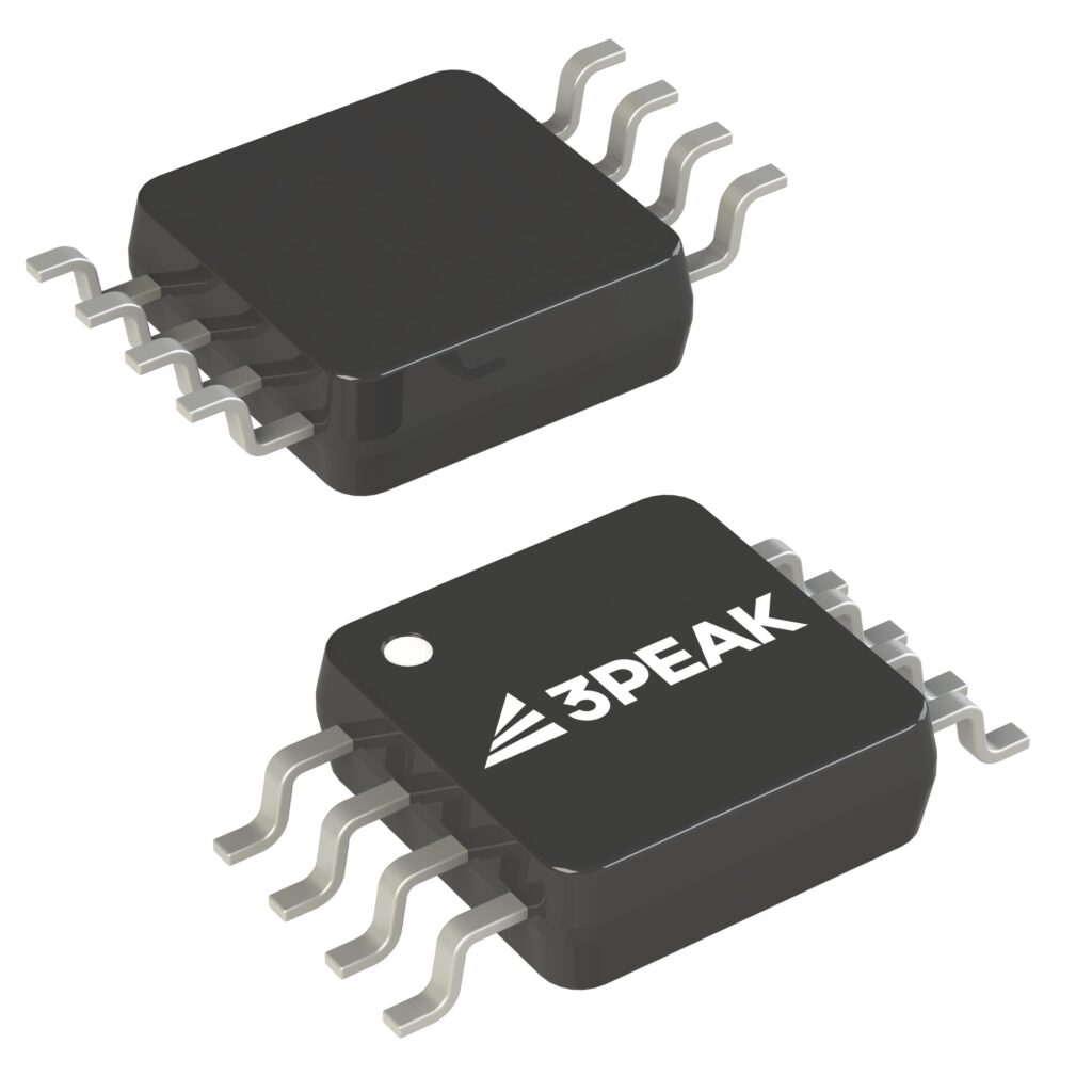
Select this component when high precision is required in automotive environments due to its low offset voltage and drift characteristics. The dual-channel configuration suits applications needing two independent amplifiers in a compact TMSOP-8 package. Consider the 470 pF maximum load capacitance limit; larger capacitors require series isolation resistors to prevent oscillation. Evaluate input crossover distortion near the upper common-mode voltage range if operating near VDD.
This part belongs to the S-19630A family of automotive-grade CMOS operational amplifiers. The 'B' designation indicates a dual-channel configuration, while 'K8T2' specifies the TMSOP-8 tape-and-reel packaging. The 'U' suffix denotes lead-free (Sn 100%) and halogen-free compliance. These devices are engineered specifically for robust performance in demanding vehicular electronic systems.
No public confirmed substitute part numbers are available in the provided documentation.
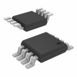 S-19630AB0A-K8T2U
The activity of extra discounts on wholesale prices is in full swing…
Please fill in your contact information and we will send you the latest wholesale price list.