ChipApex | Global Electronic Components Supplier

SEARCH
Search Product
Search Post
— IC芯片 | 连接器 | 传感器 | 被动器件 —
Search productSearch post
— IC芯片 | 连接器 | 传感器 | 被动器件 —
Consult the customer manager about the wholesale price.
consultation hotline:86-132-6715-2157
email:[email protected]
Contact the product manager for consultation. One-stop consultation is available.
Do you want a lower wholesale price? Please send us your inquiry and we will reply immediately.
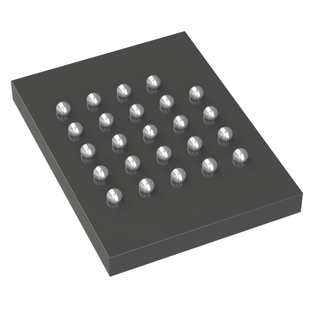
S26KL512SDABHV023 is listed in the Memory IC range at ChipApex. The manufacturer field lists Infineon Technologies. Its product description is IC FLASH 256MBIT HYPERBUS 24FBGA. Review the specifications below when checking this part for your BOM.
The Infineon S26KL512SDABHV023 is a 512 Mbit (64 MB) HYPERFLASH™ NOR flash memory device featuring the HYPERBUS™ interface. It operates with a 1.8 V core and I/O voltage, utilizing a differential clock configuration. The device supports a maximum clock rate of 166 MHz, achieving up to 333 MBps sustained read throughput via DDR data transfers. Key specifications include a 96 ns initial random read access time, uniform 256 KB sector erase capability, and an embedded ECC engine for one-bit correction and two-bit detection. It is housed in a 24-ball FBGA package.
Verify that the specific suffix 'V023' corresponds to the intended automotive grade and temperature range within the official ordering information table. Confirm the package height and ball finish requirements against the mechanical drawing. Ensure compatibility with the host controller's support for differential clocks and DCARS functionality before finalizing procurement.
Select this component when a 1.8 V supply domain is required alongside high-bandwidth read performance. The device is suitable for designs necessitating integrated data integrity features such as ECC and CRC without external processing overhead. Consider the 24-ball FBGA footprint constraints and the availability of differential clock routing on the PCB layout.
This part belongs to the S26KL/S26KS HYPERFLASH™ family, which provides CMOS NOR flash technology with a low-signal-count DDR interface. The family offers various densities and voltage options, including 3.0 V and 1.8 V variants, catering to diverse industrial and automotive memory requirements.
S26KL512SDABHI020: Identical density and interface but utilizes a 3.0 V I/O voltage level instead of 1.8 V.
The device includes an embedded Hamming ECC engine that automatically corrects single-bit errors and detects double-bit errors within each half-page during read operations.
PSC and PSC# are optional phase-shifted clock inputs used to enable the DDR Center Aligned Read Strobe (DCARS) feature, allowing independent skewing of the RWDS signal relative to the main clock.
Explore related parts through Memory, Integrated Circuits (ICs), all product categories, ChipApex homepage.
 S26KL512SDABHV023

The activity of extra discounts on wholesale prices is in full swing…
Please fill in your contact information and we will send you the latest wholesale price list.