ChipApex | Global Electronic Components Supplier

SEARCH
Search Product
Search Post
— IC芯片 | 连接器 | 传感器 | 被动器件 —
Search productSearch post
— IC芯片 | 连接器 | 传感器 | 被动器件 —
Consult the customer manager about the wholesale price.
consultation hotline:86-132-6715-2157
email:[email protected]
Contact the product manager for consultation. One-stop consultation is available.
Do you want a lower wholesale price? Please send us your inquiry and we will reply immediately.
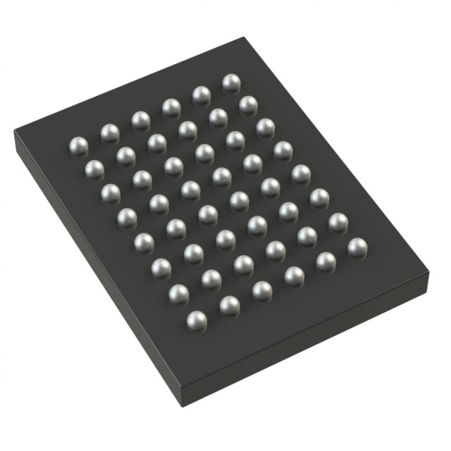
S29PL064J70BFW070 is listed in the Memory IC range at ChipApex. The manufacturer field lists Infineon Technologies. Its product description is IC FLASH 64MBIT PARALLEL 48VFBGA. Review the specifications below when checking this part for your BOM.
The Infineon S29PL064J70BFW070 is a 64-Mbit (4M x 16-bit) parallel NOR flash memory device from the PL-J series. It features simultaneous read/write architecture with zero latency, allowing independent program/erase operations in one bank while reading from another. The device supports page mode access and operates on a single 3.0 V supply (2.7 V to 3.6 V). Key specifications include a maximum access time of 70 ns and a page access time of 20 ns. It utilizes an enhanced VersatileIO (VIO) interface and includes hardware data protection features.
Verify the specific ordering suffix against the manufacturer's current valid combinations list, as availability may vary. Confirm that the package type and temperature range match the system requirements. Check for any discontinuation notices or lifecycle status updates directly from Infineon before finalizing procurement plans.
Select this component when simultaneous read/write performance is required for high-throughput applications. Ensure the system design accommodates the 48-ball FBGA package dimensions. Verify that the host controller supports the JEDEC 42.4 command set and CFI interface for proper initialization and configuration.
This part belongs to the S29PL-J family of 3.0 V Page Mode and Simultaneous Read/Write Flash memories. It is manufactured using 110-nm process technology and offers backward compatibility with older Am29F and Am29LV families. The device is designed for applications requiring reliable non-volatile storage with fast random access capabilities.
S29PL064J55BFI070
The memory space is divided into four banks (A, B, C, D), allowing up to two simultaneous operations per device. Bank A and D contain smaller sectors, while Banks B and C contain larger sectors.
The output voltage generated and input voltages tolerated on all control inputs and I/Os are determined by the voltage on the VIO pin, providing flexibility in interfacing with different logic levels.
Explore related parts through Memory, Integrated Circuits (ICs), all product categories, ChipApex homepage.
 S29PL064J70BFW070

The activity of extra discounts on wholesale prices is in full swing…
Please fill in your contact information and we will send you the latest wholesale price list.