 ChipApex | Global Electronic Components Supplier
SEARCH
Search Product
Search Post
— IC芯片 | 连接器 | 传感器 | 被动器件 —
Search productSearch post
— IC芯片 | 连接器 | 传感器 | 被动器件 —
Consult the customer manager about the wholesale price.
consultation hotline:86-132-6715-2157
email:[email protected]
Contact the product manager for consultation. One-stop consultation is available.
Do you want a lower wholesale price? Please send us your inquiry and we will reply immediately.
The SA5217D/01,118 is a 75MHz postamplifier system designed to accept low-level high-speed signals and convert them into TTL level outputs. It features an auto-zeroed first stage with noise shaping, a symmetrical limiting second stage, and a matched rise/fall time TTL output buffer. The device operates on a single 5V supply, typically consuming 40mA. It includes user-configurable input threshold and hysteresis settings to maximize signal-to-noise ratio and ensure low Bit Error Rate (BER). An auto-zero loop replaces input coupling capacitors, and a signal absent flag indicates when signals fall below the threshold.
Verify the specific ordering suffix '01,118' against the manufacturer's current documentation to confirm package type and temperature range specifications. Ensure compatibility with the intended operating voltage of 4.5V to 5.5V. Confirm that the 20-pin Small Outline Large (SOL) package dimensions align with the target PCB layout requirements before finalizing procurement.
Select this component when interfacing with SA5210, SA5211, or SA5212A transimpedance amplifiers for fiber optic applications. It is suitable for systems requiring a wideband operation up to 75MHz and programmable threshold/hysteresis levels. Consider its differential input structure for excellent power supply rejection ratio and its ability to handle long strings of identical bits in the data stream.
This part belongs to the SA521x family of optical receiver components, specifically serving as the postamplifier stage. It is designed to work in conjunction with preamplifiers like the SA5210/5211/5212A to convert photodetector currents into standard digital TTL levels. The device represents a 'system on a chip' solution for high-speed optical communication links.
The SA5214 is noted as a related device; however, it differs by providing access to internal amplifier stages A1 and A2, whereas the SA5217 focuses on the A2 output and A8 input for Schmitt trigger activation.
It utilizes an auto-zero loop connected to pins CAZP and CAZN, which cancels the DC offset from the transimpedance amplifier and the SA5217 itself, eliminating the need for input coupling capacitors.
The FLAG pin is a digital output that goes LOW when data is present above the threshold. When HIGH, it indicates a low signal condition, which can be used to jam the data output if connected to the JAM pin.
Yes, the threshold voltage and hysteresis voltage range are user-configurable using external resistors connected to the THRESH and RHYST pins, respectively.
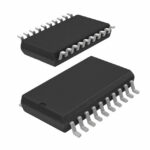 SA5217D/01,118
The activity of extra discounts on wholesale prices is in full swing…
Please fill in your contact information and we will send you the latest wholesale price list.





